1) Try to confirm the dip switch settings, the NA103 card is different then in the manual I attached I attached in a previous message.Hi na103! I'm glad you're joining the discussion, the more the better
If you ask me, a modern re-engineering of the Rambow (lol) would be amazing. The only thing, it seems to me, that really limits the 100A is the memory size, and the only thing causing that is a scarcity of the OG solutions like the original "8087" memory expansion card. Please, go for it, and happy to help in any way!
As far as the dip switch settings on the 100B card go, na103 you indicate that switches 1-3 are used for banks 1-3 activation, whereas N. Brown earlier indicated that switch 1 was parity on/off and 2-4 were banks 1-3 on/off, if I'm understanding correctly. Is this a difference in your re-engineered card, or were there simply variations in the original designs? Do we know? I don't know if the card I'm using is the same original card as what you were using for your reverse engineering.
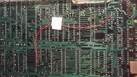
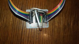
N.Brown -- I wouldn't mind trying out the mod you indicated: "wire the 8251 USART pin 24 the /DTR signal back into the chip that generates the INTL signal on its Data bit 5 pin" as being a simple non-destructive mod. Do you happen to know on the chip placement diagram which two chips these are? I wasn't sure (wow if we had full schematics of the 100A it would be VERY handy). I also think socketing E104 is a good plan, as also being non-destructive (If I don't mess it up lol).
N.Brown -- thank you for the huge amount of information; I'm still digesting it. What I think I'd like to try is:
1) Try to confirm the dip switch settings if we can
2) Do the 8251 mod
3) Socket E104
4) connect A16-A18 directly to the memory expansion rather than inverted
5) connect A19 if step 4 works (or perhaps even if it doesn't) -- or try just pulling it high as you suggest.
6) put everything back to stock and use na103s re-engineered solution! (which yes would be, as I said, AMAZING to have in the world).
Let me know if this seems sensible, or if I've missed something?
Cheers all! A
")
In theory of the 100B model you should bet a error message about party error checking with either the first switch 1 or the last switch. Then you might have to go through both schematics to verify which one closest matches yours.
In the list above you forgot about the IO//M signal line replacing the Shared/noshared signal at the memory expansion connector on the 100A.
If your number 4) fails try pulling A19 high, then if nothing try pulling A17 alone on the memory expansion card high. This will change the memory origination on the card.
..
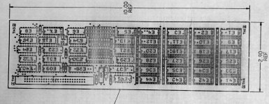
On the Rb100A_component layout
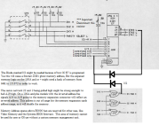
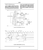
IC E87 a 8251A USART chip pin 24 the DTR signal to pin 8 IC e72 a 74LS244 on the D3 input line which should outputted on pin 12 as BAD3 signal. Of course you must cut the ground signal connected to pin8 of IC e72.
This modification should be available some here on the internet, if it hasten be removed.
..
6) might be your end solution , but a couple years ago I did try to contact the author directly at github.com for the RB100A version of the memory expansion card. but never got a reply.
It was probably got marked as Spam or something like that.
..
Sorry to put you through this, but the old version of the card we where able to modify for use with the 100A and or plus models at one time, including versions that did not have the PLA on board.
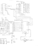
A durity /hard to read copy of the RB100A schematics can be found @ http://www.bitsavers.org/pdf/dec/rainbow/MP-01491-00_PC100_Print_Set_198212.pdf
(If I you mess it up lot, please let me know as I still have 3 extra RB100A models sitting around as part units for on going maintenance contracts, since I open up my big mouth in the first place. ).
..
Attachments
Last edited: