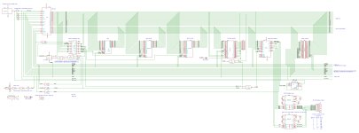
Out of curiousity about the architecture, why the double buffering? You're pushing a huge amount of potential current there through multiple buffers - eg, One for the CPU, and one for each card.
The z80 can push a few milliamps - the datasheet says 1.5 high and 2.5 low IIRC, or thereabouts, but that seems related to thermal dissipation rather than actual limits. In the ZX Spectrum architecture, it directly drove against signals at 3.5 MHz with a load of 330 Ohms where they were used as bus separators ( rather than using a buffer where it was actually needed to separate busses ), or around 15 mA at 5v - both high and low. Looking at the signals on a scope tells you it's feeling the load, and the CPU gets warm, but it handles it, even though this is clearly operating at a low duty cycle, but it has a lot more push than most people realize.
You're interfacing with CMOS RAMs, and other similar chips, so the z80 itself probably wouldn't even blink at the requirements to drive around 20 chips directly from the bus, and if using the bus buffering, you're pushing around 12 to 25 mA per output line within data sheet specifications ( 74LS244 ) - so the extent of buffering may not be necessary.
I know some other systems buffer everything from the CPU, but mostly on systems that share data and address lines, so there was a need for external latches and buffers to separate this information in the time domain.
If you're buffering the cards directly, the z80 could easily handle a half-dozen slots without needing a local bus buffer. Hence I'm curious as to the buffer near the CPU and a buffer at each card as well.
I have seen z80s fail, but it's pretty rare. The larger chip surface area gives pretty good cheat dissipation at lower clock speeds so it really makes me curious as to how many cards the architecture is designed to take?