I see you are using a bidirectional buffer now, rather than the LS244 you previous had for read - You could also eliminate the 244 at U14 if you extended the circuit, but I'll leave that decision for the future. I assume all of the latches are holding correctly, and you've already confirmed through pattern testing that there's no cross-talk there or false setting of a latch.
Right now, you have a fair bit going on. Some troubleshooting tests you can consider;
1) Write a ROM with a test pattern or just data and replace a RAM chip with a ROM chip - You might need to make up a socket to adapt the different pins, and program in a 16K pattern 4 times into a 27c256 or 8 into 27c512 due to the A14/A15 mismatch, but that's enough for a test... This way you can test reading of a chip with certainty. If you can read back the ROM chip correctly, then at least you can be confident it's not a read issue. Don't forget to remove the other RAM chips from the board first, as a faulty RAM chip can interfere with operation. ( I assume likewise you are only testing with a single RAM chip to avoid the possibility of a faulty RAM or a ram with enable issues interfering with the bus )
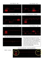
2) Get a logic analyser - you can record several seconds of interactions with the chips and zoom straight into the output to see what is going on - They cost about US$7 for an 8 channel model that comes with excellent software and will run at up to 24 Msps, which will give you sub-clock timing for a z80... At around 12 Msps, you can probably record for several seconds of testing over a USB. A problem with data stability is very hard to troubleshoot without a logic analyzer. I recently bought the Hantek 32 channel analyser and it works great.
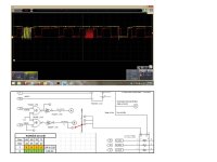
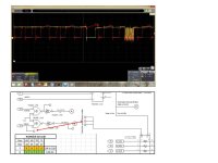
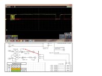
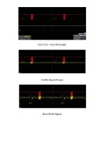
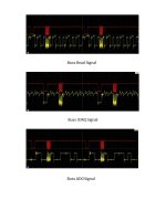
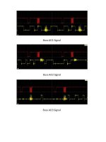
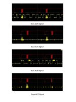
3) Once you've confirmed you can read a ROM in a RAM socket reliably, then you only need to focus on the WRITE operation testing. You can also do this with just a two channel scope by triggering on the MEMORY select line from the 138 (U12) on the negative edge, and examine what other signals are doing at the same time since the recent circuit changes made sure that the memory chips are all enabled by this line. You can check data lines ( all set to what you're putting out) and other signals such as buffered RD/WR, direction, etc and make sure they are all where they are supposed to be.
This should be enough to find the exact cause of your problem. Without narrowing down the cause, then you're struggling to guess where the issue is. Now that you've eliminated them, the previous race condition and multiple chip enables were clearly not enough to stop the design from working, but there's only so much desktop troubleshooting you can do without a better way to look into what is going on
")
Regards
David