• Please review our updated Terms and Rules here

RAMdisk under CP/M 2.2

If you think this may be helpful, I can reprogram the CPLD of a RAM/ROM512K board to emulate your design. https://www.retrobrewcomputers.org/doku.php?id=builderpages:plasmo:rr512k:rr512k_rev1

The memory can be two RAM devices up to 512K each and the CPLD has plenty of resources to emulate your logic. The propagation delay will be very different, but at least it can check out your logic and your test software. I can check out the modified board using a RC2014-compatible Z80 single board computer.
Bill
 
Doug, I hear you. I used to use those and the nylon ones for keep pins in line. I used to making wire-wrap wiring changes on very packed chassis used in submarines. I never took to the powered tools. Other than refering to them once as a 'wire wrap gun' when asked what that odd looking thing was in my carry-on as I was going through the San Francisco airport back in the early 80s. Probably not my best choice of words. All kidding aside, I do suspect there is some intermittent or cold solder joint somewhere. These protoboards are NOS off of eBay, so...... Well, off to genning up a new board!
 
It's a complex problem - and for the life of me, I can't work out why it's only happening on read - the closest idea I could come up with was something like RD shorting to a bus gate control like in such a way to cause self-oscillation - eg, a feedback loop -= I really can't think of anything else that would cause high frequency oscillations that look to be an order of magnitude or more above the clock frequency in a logic system. It's like one of the lines ( probably read ) is shorted somehow to another line, and then loops back on itself, so that it shorts, resets, shorts, resets, and so on. Generally the scope image you're seeing can't be created by missing grounds or other signals and I've also seen data lines provide VCC or GND to a chip before through the diode protection network on each pin. But in your case, the oscillations look to be occuring at a higher frequency than the scope quantisation period can handle - ie, a digital logic feedback mechanism. 1

Can you get a higher scan rate image of on of the messed up signals? eg, at 100us per division? Determining the frequency of what you're seeing is a clue also.

Honestly, if you can get to it, run a wire to the same pins on the z80 - I'm pretty sure the signal should be clean there. If it's not, then the z80 is at fault ( Fan out issue maybe? ) - If the z80 is stable, then trace the line through the PC all the way to the card bus and see where the oscilations are first noted, get induced or otherwise start.

Building another card with just the 138 wired up to begin with is as you are suggesting, so that you can generate and test the signals directly before RAM is installed as you proposed is also a good idea.

Your premise and design appear correct, and the use of the logic circuits is also good. The only parallel race condition you had was eliminated, so I think solving the oscillation on read problem is all that's standing between you and a working RAM disk.

I wondered why you were using wire wrap so extensively, and now it makes sense - thanks for sharing the background story there -
David.
 
Well, I have lot's of wire-wrap wire, and sockets, and lot's of chips, and a lot of time (retired). And I kind of have lots of experience way back when. Heck, my first PC back in the ealy 80s was a wire-wrap S-100 based clone of a TRS-80 Mod 1 Lev II machine. As for the noise/spikes, I did expand one that I found. It looks like the read line goes low for about 1.5 us based on the scope trace. I expanded one of them and counted 11 pulses, each of equal duration. If my calculations are close, that comes out to about 7,333,333 Hz.
 
That's a weird frequency - Too slow for typical feedback oscillators and too fast for anything that's clocked on your board if your maximum clock rate is 2 MHz.

Have you checked the z80? I know it's a weird idea, but I assume you've tied all the control lines, eg, BUSRQ, high with a reasonably strong resistor? eg, around 4.7K max? If the oscillations are at the z80 and your control lines aren't floating, then it's probably a faulty z80.
 
If you think this may be helpful, I can reprogram the CPLD of a RAM/ROM512K board to emulate your design. https://www.retrobrewcomputers.org/doku.php?id=builderpages:plasmo:rr512k:rr512k_rev1

The memory can be two RAM devices up to 512K each and the CPLD has plenty of resources to emulate your logic. The propagation delay will be very different, but at least it can check out your logic and your test software. I can check out the modified board using a RC2014-compatible Z80 single board computer.
Bill
Bill, that could be useful, except I would have no way to implement it on the protoboards I currently have which are all DIP based. Frankly I have never used GAL/PAL type devices.
 
That's a weird frequency - Too slow for typical feedback oscillators and too fast for anything that's clocked on your board if your maximum clock rate is 2 MHz.

Have you checked the z80? I know it's a weird idea, but I assume you've tied all the control lines, eg, BUSRQ, high with a reasonably strong resistor? eg, around 4.7K max? If the oscillations are at the z80 and your control lines aren't floating, then it's probably a faulty z80.
Well, since the printer card and the dual port serial card work without any issues..... I already wired up another card with the minimum circuitry, I;m going to test that tomorrow. If it works, I'll add stuff piece by piece and see where that takes me.
 
Update: I have started to build up a new board, using the exact same design, although I have made slight changes in some of the chip locations. And so far, the write and read low pulses have been rock solid perfect. I attached the schematic and all of the wires in green, and the associated chips, have been installed to this point. The next phase of this will be the wiring between the '244 and the three '374s, and then another test. Stay tuned to your local station for breaking news......
 

Attachments

  • MemoryDiskv7(test).pdf
    91.9 KB · Views: 5
Update: I have started to build up a new board, using the exact same design, although I have made slight changes in some of the chip locations. And so far, the write and read low pulses have been rock solid perfect. I attached the schematic and all of the wires in green, and the associated chips, have been installed to this point. The next phase of this will be the wiring between the '244 and the three '374s, and then another test. Stay tuned to your local station for breaking news......

Given what you already eliminated, it's going to be a really interesting problem if your new board exhibits the same activity... Well, I am going to guess on the side of "It will probably work this time" - :)

As an experiment, can you plug in two boards at the same time? I would be really curious to note whether having both boards installed caused the same issue on the new board. You would need to disable or unplug the 245 on the original board to avoid bus conflict, but I'd be really curious as to how this affected the new board, since it would load up the PSU and bus the same as the original board, and let you test for fan-out related issues as you progress.

David.
 
Well, so far I have every line wired except the wires to the RAM chips themselves and the read & write lines look perfect. I mean they are rock solid. Tomorrow I'm going to wire up all the lines within the RAM array, and then slowly tie them into the rest of the circuit and test along the way. Yep, I agree, there looks to be something with how I put together the original board. Time will tell.
 
Well, I completed wiring up the data lines to all of the RAM chips and the test run still shows rock solid signals. Granted, the test ran without any RAM chips installed. Next is to wire up the address lines to the RAM chips and run the test. Followed by the CS, read and write control signals to the RAM chips. and finally with the RAM chips installed. That is gonna take a few days to get done.
 
Well, the write & read pulses were picture perfect when running the tight loop test, writing and reading FF to one location of one chip. Were being the operative word. Perfect up until the Read lines (pin 22), the Write lines (pin 27), and each of the Chip Select lines (pin 20) were wired up. And now the noise and spike are back on the enable (pin 19) of the data bus transceiver. I was sure not expecting that. So, the next step is to remove all of the read, write, and chip selects, and just run them to the first RAM chip to see if that works...... This sure is a weird one.
 
1) I took out all but the chip select for RAM ), still spikes & noise. Took out all of the read lines, still spikes & noise. Took out the write signals, and the noise & spikes go away...... ?????
2) Put back all the chip select lines. no noise or spikes
3) Put back all the write lines (no read lines connected), and noise & spikes are back..... ?????
4) Put back all the read lines (no write lines connected), and noise & spikes are gone....
 
Could you be exceeding fan-out on one or more of the signals?

Well, I'm wondering...... But if it was a fan-out issue, pulling all but one RAM chip should make that go away.....

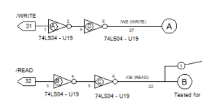
But it looks like I have uncovered yet another artifact of this problem. A system reset doesn't clear it????? A POR will clear it though. Which it implies something is going into oscillation..... But what is; and how and why..... I'm half tempted to swap out the 74LS02 at U16 and replace it with a 74LS04. As in.....

1682638857489.png
 
But IIRC, wasn't the oscillation on the bus (computer) side of the circuit? and the circuit is responding correctly to the oscillation?

You might need to look at the processor side of the equation a little further -
 
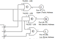
And even change the '374 latch control decode to this:

1682639376875.png

At this point, I guess I'm just 'shotgunning' to find something that fixes things. This circuit is not complicated and should not be this difficult. At least making these changes should simplify it some. I can't see it being a soldering issue or a cut or broken wire, given this is a complete new build......
 
But IIRC, wasn't the oscillation on the bus (computer) side of the circuit? and the circuit is responding correctly to the oscillation?

You might need to look at the processor side of the equation a little further -

I think the oscillation is internal. Once I reset the system, it works just fine. I can do the stuff I could always do. Run CP/M, etc. So it looks like the oscillation, if that what it really is, is internal to the circuitry on this board.
 
I'll make the circuit changes I mentioned next. and if still no luck, then I will start probing each of the bus pins to see the before and after effects of causing the failure. Maybe that shows something.....
 
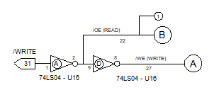
I'm also wondering if maybe re-configuring the read and write signal to where the read signal to the RAM chips is really just an invert of the write line. As in:

1682692582155.png
 
Back
Top