• Please review our updated Terms and Rules here

Setting up a DECnet network with a Pro380 and Windows client?

I took a quick look. It exits with EMT 0. This happens at 2530. The error code is reported at 2522 so the error code is stored into 2064.

At 2660 is stores 10 octal into 2064. It seems to test bit positions in 2062 and produce error codes. But I cannot find directly where 2062 is loaded.
 
When I said that you could use Xhomer I meant my fork of Xhomer since I have instrumented the code with a tracing-facilty that give a more detailed log than the original. You can find it on my github. Compile it with tracing enabled.


Out of curiosity I checked a bit more:
The entry point might be at 2054 (BR 2200) or 2052. I wonder if the value at location 24 is indicating the starting point? The BR jumps past all the local variables.

At entry R0 is the slot ID. R0 is stored on stack and then ends up in 2060 as you discovered.

Why doesn't SIMH disassemble line 2454 and 2574? I.e 072127 and 072527.
If I read it correctly it is supposed to be ASH instructions, shifting R1 and R5 respectively. The number of shifts is 27 octal which is 23 decima!? Why shift 23 steps left on a 16 bit register?

Regarding the 2062: I think that is just a static bitmask to set which tests to actually test. It goes away doing a JSR 3776 and is then evaluating the result. The subroutine at 3776 does a EMT 5 which is used by the memory diag ROM as well. This EMT sets up the memory mapping so that on board memory can be mapped in. It looks like it maps this memory at the 3 meg boundary. Without checking in detail what this routine does it seems like it does a memory test which points towards that you have a problem with the onboard memory.
 
While searching for RAM memory speed, I discovered the daughterboard schematics and notes are in the PRO 350 print set. There are two jumpers on the 350 daughterboard for 128K and 512K. I don't know if the 380 daughterboard is identical, but it seems likely with just the jumpers set.
View attachment 1277914View attachment 1277915
I added this upgrade to my Pro 350. Easy-peasy if you are careful. I would be super interested in a DECNA. There were three of them that showed up on eBay last month - all in the wee hours of the night and all gone by the time morning coffee was ready. Bummer.
 
The small daughtercards on the PRO 350 (are those the same on the 380?) can easily be changed to 512 k modules by replacing the 64kbit chips into 256 kbits. I don’t remember if you need to change a jumper or so as well. I did this mod 30 years ago. I think it is possible to find 256 kbit chips on Ebay or possibly someone here has a bunch of them.

I don’t know about the CTI bus memory expansion. The firmware has a bug so that it will never handle more than 512 k.
Simple jumper, easy to do. I recommend using an IR pre-heater to warm up the board, then either hot air or a nice soldering iron to desolder the chips. To be honest though just cutting the leads and pulling the pins one by one is a heck of a lot simpler. Then clear the holes with wick (easy if board is already pre-heated) drop in 16 DIP sockets, solder and plug in RAM.

Now for *real* interesting things, the Pro/380 does have an additional 4 address bits on an extended socket there so you can build a board that can do 2mb or 4mb on a board. There have been rumblings that you can't run more than 2mb memory on POS, no practical way to test it without 4 memory boards, a DECNA for that last 128k and the disk controller....
 
Interesting limit. I wonder why 3mb as opposed to 2 or 4. The IO page can't be that big on a Pro :)

Note: I'll try to take pics tonight after work, have to go to Chicago for 2 days in the early morning.
 
Last edited:
When I said that you could use Xhomer I meant my fork of Xhomer since I have instrumented the code with a tracing-facilty that give a more detailed log than the original. You can find it on my github. Compile it with tracing enabled.


Out of curiosity I checked a bit more:
The entry point might be at 2054 (BR 2200) or 2052. I wonder if the value at location 24 is indicating the starting point? The BR jumps past all the local variables.

At entry R0 is the slot ID. R0 is stored on stack and then ends up in 2060 as you discovered.

Why doesn't SIMH disassemble line 2454 and 2574? I.e 072127 and 072527.
If I read it correctly it is supposed to be ASH instructions, shifting R1 and R5 respectively. The number of shifts is 27 octal which is 23 decima!? Why shift 23 steps left on a 16 bit register?

Regarding the 2062: I think that is just a static bitmask to set which tests to actually test. It goes away doing a JSR 3776 and is then evaluating the result. The subroutine at 3776 does a EMT 5 which is used by the memory diag ROM as well. This EMT sets up the memory mapping so that on board memory can be mapped in. It looks like it maps this memory at the 3 meg boundary. Without checking in detail what this routine does it seems like it does a memory test which points towards that you have a problem with the onboard memory.
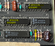
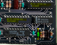
The thought did cross my mind, which got is why I started looking at the memory chips used by DEC and the access time. Recall, I also have a memory card that does not work for an unexplained reason. Oddly, the DEC part numbers for the memory chips on those two boards are of the -02 version, while the memory chips on the memory cards that do work are of the -01 version. The -02 version is not listed in the Pro350 Print Set. Probably just a coincidence and maybe not significant.
 
I added this upgrade to my Pro 350. Easy-peasy if you are careful. I would be super interested in a DECNA. There were three of them that showed up on eBay last month - all in the wee hours of the night and all gone by the time morning coffee was ready. Bummer.
There were actually four cards. I got one of them, but unfortunately it is not working in my 380.
 
I replaced the two socketed chips (Intel Ethernet controller C82586) and Fujitsu Ethernet encoder (MB502A) on a lark with no luck. Same error. If I assume the board does not have a defect, the LS logic chips are pretty rugged and I wouldn't think they have gone bad. I eliminated the controller. The shared memory seems like a logical culprit. I don't know about that big square ceramic chip with the clamp. I am not sure how that chip comes off. It looks like the clamp is bent under the socket. No part number that I can see, but there are some numbers running under the clamp that look like the year and week production run (8344).
 
I replaced the two socketed chips (Intel Ethernet controller C82586) and Fujitsu Ethernet encoder (MB502A) on a lark with no luck. Same error. If I assume the board does not have a defect, the LS logic chips are pretty rugged and I wouldn't think they have gone bad. I eliminated the controller. The shared memory seems like a logical culprit. I don't know about that big square ceramic chip with the clamp. I am not sure how that chip comes off. It looks like the clamp is bent under the socket. No part number that I can see, but there are some numbers running under the clamp that look like the year and week production run (8344).
The big chip is a dual memory DRAM controller. It both handles DRAM refresh and RAS/CAS as well as dual port arbitration. Intel 8207.
 
Interesting limit. I wonder why 3mb as opposed to 2 or 4. The IO page can't be that big on a Pro :)

Note: I'll try to take pics tonight after work, have to go to Chicago for 2 days in the early morning.

Remember that for examle both DECNA and the video card takes up space in this area. DECNA uses 128k. Don’t remeber the memory window of the video board. Then there might be other boards that need IO. It adds up. The Diag ROM for the memory board cleraly show that it will configure memory up to the three meg limit.
 
I've done some work with the DECNA boards (I wrote a DECNA emulator for an Xhomer fork that more or less works -- it even booted disklessly). So I had to do a bunch of reverse engineering.
The diagnostic ROM runs through 10 separate tests at its start:
  1. Test1: tests the ID ROM (which contains the MAC address) and does some initial testing on the dual-ported RAM. When it fails for the following reasons it yields the following codes (numbers are in octal):
    1. Failure 001: bus error reading ID ROM
    2. Failure 002: inconsistency in ID ROM contents: checksum invalid, MAC address is all 0s, bit 0 in the second MAC word is 1.
    3. Failure 003: failure to map dual ported RAM to physical address 0o05000000
    4. Failure 004: readback on MEM register isn't 012, inverted (using COMB) MEM register doesn't read back properly, write of 007 to MEM register doesn't read back, inverted (using COMB) MEM register doesn't read back properly. When this part succeeds it leaves the dual-ported RAM mapped at 0o14000000
    5. Failure 005: attempt to write first word of the dual-ported RAM yields a bus error
    6. Failure 006: *failure to see a bus error* when clearing ME in CTL and repeating test from previous step. After this step the DP RAM is unmapped.
  2. Test2: tests the dual ported RAM in earnest. This test maps the 128 KiB DP RAM to physical address 0o14000000..0o14377777 and turns on access in the CTL register.
    1. It then maps 4 pages (32 KiB) at a time of the DP RAM to virtual address space 020000..117777. It repeats this, moving the 32 KiB window over the 128 KiB of DP RAM on the board. For each of these mappings it does a series of tests. If any of these tests fails it posts failure codes 010 (for DP RAM offsets 0300000..0377777), 011 (for DP RAM offsets 200000..277777), 012 (for DP RAM offsets 100000..177777), or 012 (for DP RAM offsets 000000..077777)
    2. It then waits for a bit and back to read the first word of shared RAM and makes sure it's the pattern it last wrote (052525). If it's not then it posts error 013. On successful completion it leaves the highest 8 KiB of DP RAM (PA 0o14360000..0o14377777, which corresponds to DP RAM offsets 0360000..0377777) mapped at virtual address 020000...037777).
I haven't really worked through the details of the remaining 8 tests.

Concerning the discussion of the CTI option ROM: the DECNA actually contains 2 completely separate position-independent code blocks: the diagnostic ROM and the network boot ROM (to boot a diskless client system).
Every CTI option ROM starts with the following header:
OffsetSizeMy nameValue on DECNADescription
000wordID0000042The CTI board ID. Because the CTI option ROM is read byte at a time boards that don't implement a real ROM will simply return a single byte for the ID and everything else (e.g., 004 for the floppy controller). Because the ID is a 16-bit word, in such a case the byte is read twice (e.g., 004 * 0400 + 004 = 002004). This is why all the non-ROM CTI boards have IDs with the same high and low bytes.
002wordMAGIC0125377This is a pattern that the system boot ROM will recognize as indicating that the CTI board actually has a ROM.
004byteFLAGS004I'm guessing this is flags. The DECNA board is the only one with a non-zero value in it, so I'm guessing 004 means "bootable".
005byteNSECS002The number of sections (and section headers) to follow.
006wordROMSIZ000040The overall size of the ROM, in bytes, divided by 256.
010word?000000All zero. I'm not sure what this is.

This is then followed by the two section headers:
ROM offsetHeader offsetSizeMy nameDECNA value
Description
0120005 wordsSECTYP0042046, 0000000, 0000000, 0000000, 0000000Identifies the section type. 0042046 just happens to be "&D", and this section is the Diagnostic section. Other possible values are 00410046 + [0]*4 ("&B") for boot sections, 00530046 ("&V") for I have no idea, and 00500046 ("&P") also for something I don't know.
0240123 bytesSECOFF000000052ROM byte-offset of the beginning of this actual section.
027015wordSECLEN0012040Size (in bytes) of section
031017byte-0Must be 0


0320005 wordsSECTYP0041046, 0000000, 0000000, 0000000, 0000000Boot ("&B") section ID
0340123 bytesSECOFF000012112ROM offset of the beginning of this actual section.
037015wordSECLEN0003742Size (in bytes) of section
041017byte-0Must be 0

So the diagnostic code you want to disassemble starts at ROM byte offset 000000052. I'm attaching a very raw and barely annotated disassembly that I've worked from.
Note that the last word of each of these two sections contains a dedicated checksum word that covers its contents, and similarly the entire ROM ends with a checksum word that covers the whole thing.
The system boot ROM will load the entire contents of a CTI option ROM section (up to 0o60000 bytes worth) at RAM location 02000 and it will then jump to that first location.
Before making the jump the system boot ROM sets up R1 with the CTI slot number (0..5 for the PC325/PC350, 0...6 for the PC380) and makes the jump. The system ROM provides some support code that is accessible via EMTs:
EMT numberMy nameInputsOutputsDescription
0CTRSMNoneNoneDoesn't return. Resumes back in the system boot ROM.
1CTFINDR0: CTI card ID (e.g., 0000042)R0: CTI slot index 0..6 or -1 on failureLooks through the soft configuration data to see if it has seen the given CTI card ID. Returns the slot number if it finds such a card, -1 on failure.
2ICENBR1: (Interrupt controller # (0..2) << 6 | interrupt channel (0..7))NoneExecutes "Clear Single IRR and IMR" for the given controller and channel. This enables the given interrupt.
3ICDISR1: (Interrupt controller # (0..2) << 6 | interrupt channel (0..7))NoneExecutes "Set Single IMR Bit" for the given controller and channel. This disables the given interrupt.
4ICTSTR1: (Interrupt controller # (0..2) << 6 | interrupt channel (0..7))NoneExecutes "Set Single IRR Bit" for the given controller and channel. This creates a software-generated interrupt.
5KMAP-4(sp) number of 8 KiB pages to map (0..4)
-2(sp) High 9 bits of physical address.
NoneStores KIPAR1-4 into 01120, 01116, 01114, 01112, and then reprograms them to map the required space. Also sets bit 04000 in the UIPAR0 to indicates that KIPAR1-4 are stored in RAM.
6KUMAPNoneNoneRestores KIPAR1-KIPAR4 from values stored in 01120, 01116, 01114, 01112 only if bit 04000 is set in UIPAR0. Then clears bit 04000 in UIPAR0.

Hopefully that will give you more information to help you decode what's going on in the diagnostic ROM.
If you get further into it you'll need http://bitsavers.org/components/intel/ethernet/i82586.pdf and an app note in http://bitsavers.org/components/intel/_dataBooks/1991_Microcommunications.pdf (pp. 1-337 to 1-417).
IIRC you should be forewarned: the datasheet is actually wrong in several important places. Off the top of my head I seem to recall it is wrong about the top-level shared RAM structure used by the i82586. The top-level "System Configuration Pointer" in the block at the last 10 bytes of memory does not point to the system configuration block (SCB). Instead, it points to something called an "intermediate system configuration pointer" (ISCP) which then points to the SCB. This is mentioned in the app note. Ugh.
--Bjoren
 

Attachments

  • decnadiag.mac.txt
    135.1 KB · Views: 6
I think the DECNA memory is "real" memory and is mapped for general use. From what I saw in a technical document the issue was a stock Pro/350 with 512k of memory doesn't have enough to run the Decnet stuff, so they made sure you would with a bit of memory.

However it's possible that they wanted to use more space than the IO page for stuff, so did a Vax thing and blocked off 1/4 of the memory.

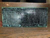
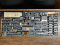
Anyway I took a few pics before jetting off here. These are low res versions, will upload better ones later. However I think the label is the MAC address, and mine does NOT have any wirework.

Let me know if there's a diff between mine and yours.

C
 

Attachments

  • IMG_1024.JPG
    IMG_1024.JPG
    1.5 MB · Views: 6
  • IMG_1026.JPG
    IMG_1026.JPG
    1.2 MB · Views: 6
I've done some work with the DECNA boards (I wrote a DECNA emulator for an Xhomer fork that more or less works -- it even booted disklessly). So I had to do a bunch of reverse engineering.
The diagnostic ROM runs through 10 separate tests at its start:
  1. Test1: tests the ID ROM (which contains the MAC address) and does some initial testing on the dual-ported RAM. When it fails for the following reasons it yields the following codes (numbers are in octal):
    1. Failure 001: bus error reading ID ROM
    2. Failure 002: inconsistency in ID ROM contents: checksum invalid, MAC address is all 0s, bit 0 in the second MAC word is 1.
    3. Failure 003: failure to map dual ported RAM to physical address 0o05000000
    4. Failure 004: readback on MEM register isn't 012, inverted (using COMB) MEM register doesn't read back properly, write of 007 to MEM register doesn't read back, inverted (using COMB) MEM register doesn't read back properly. When this part succeeds it leaves the dual-ported RAM mapped at 0o14000000
    5. Failure 005: attempt to write first word of the dual-ported RAM yields a bus error
    6. Failure 006: *failure to see a bus error* when clearing ME in CTL and repeating test from previous step. After this step the DP RAM is unmapped.
  2. Test2: tests the dual ported RAM in earnest. This test maps the 128 KiB DP RAM to physical address 0o14000000..0o14377777 and turns on access in the CTL register.
    1. It then maps 4 pages (32 KiB) at a time of the DP RAM to virtual address space 020000..117777. It repeats this, moving the 32 KiB window over the 128 KiB of DP RAM on the board. For each of these mappings it does a series of tests. If any of these tests fails it posts failure codes 010 (for DP RAM offsets 0300000..0377777), 011 (for DP RAM offsets 200000..277777), 012 (for DP RAM offsets 100000..177777), or 012 (for DP RAM offsets 000000..077777)
    2. It then waits for a bit and back to read the first word of shared RAM and makes sure it's the pattern it last wrote (052525). If it's not then it posts error 013. On successful completion it leaves the highest 8 KiB of DP RAM (PA 0o14360000..0o14377777, which corresponds to DP RAM offsets 0360000..0377777) mapped at virtual address 020000...037777).
I haven't really worked through the details of the remaining 8 tests.

Concerning the discussion of the CTI option ROM: the DECNA actually contains 2 completely separate position-independent code blocks: the diagnostic ROM and the network boot ROM (to boot a diskless client system).
Every CTI option ROM starts with the following header:
OffsetSizeMy nameValue on DECNADescription
000wordID0000042The CTI board ID. Because the CTI option ROM is read byte at a time boards that don't implement a real ROM will simply return a single byte for the ID and everything else (e.g., 004 for the floppy controller). Because the ID is a 16-bit word, in such a case the byte is read twice (e.g., 004 * 0400 + 004 = 002004). This is why all the non-ROM CTI boards have IDs with the same high and low bytes.
002wordMAGIC0125377This is a pattern that the system boot ROM will recognize as indicating that the CTI board actually has a ROM.
004byteFLAGS004I'm guessing this is flags. The DECNA board is the only one with a non-zero value in it, so I'm guessing 004 means "bootable".
005byteNSECS002The number of sections (and section headers) to follow.
006wordROMSIZ000040The overall size of the ROM, in bytes, divided by 256.
010word?000000All zero. I'm not sure what this is.

This is then followed by the two section headers:
ROM offsetHeader offsetSizeMy nameDECNA value
Description
0120005 wordsSECTYP0042046, 0000000, 0000000, 0000000, 0000000Identifies the section type. 0042046 just happens to be "&D", and this section is the Diagnostic section. Other possible values are 00410046 + [0]*4 ("&B") for boot sections, 00530046 ("&V") for I have no idea, and 00500046 ("&P") also for something I don't know.
0240123 bytesSECOFF000000052ROM byte-offset of the beginning of this actual section.
027015wordSECLEN0012040Size (in bytes) of section
031017byte-0Must be 0


0320005 wordsSECTYP0041046, 0000000, 0000000, 0000000, 0000000Boot ("&B") section ID
0340123 bytesSECOFF000012112ROM offset of the beginning of this actual section.
037015wordSECLEN0003742Size (in bytes) of section
041017byte-0Must be 0

So the diagnostic code you want to disassemble starts at ROM byte offset 000000052. I'm attaching a very raw and barely annotated disassembly that I've worked from.
Note that the last word of each of these two sections contains a dedicated checksum word that covers its contents, and similarly the entire ROM ends with a checksum word that covers the whole thing.
The system boot ROM will load the entire contents of a CTI option ROM section (up to 0o60000 bytes worth) at RAM location 02000 and it will then jump to that first location.
Before making the jump the system boot ROM sets up R1 with the CTI slot number (0..5 for the PC325/PC350, 0...6 for the PC380) and makes the jump. The system ROM provides some support code that is accessible via EMTs:
EMT numberMy nameInputsOutputsDescription
0CTRSMNoneNoneDoesn't return. Resumes back in the system boot ROM.
1CTFINDR0: CTI card ID (e.g., 0000042)R0: CTI slot index 0..6 or -1 on failureLooks through the soft configuration data to see if it has seen the given CTI card ID. Returns the slot number if it finds such a card, -1 on failure.
2ICENBR1: (Interrupt controller # (0..2) << 6 | interrupt channel (0..7))NoneExecutes "Clear Single IRR and IMR" for the given controller and channel. This enables the given interrupt.
3ICDISR1: (Interrupt controller # (0..2) << 6 | interrupt channel (0..7))NoneExecutes "Set Single IMR Bit" for the given controller and channel. This disables the given interrupt.
4ICTSTR1: (Interrupt controller # (0..2) << 6 | interrupt channel (0..7))NoneExecutes "Set Single IRR Bit" for the given controller and channel. This creates a software-generated interrupt.
5KMAP-4(sp) number of 8 KiB pages to map (0..4)
-2(sp) High 9 bits of physical address.
NoneStores KIPAR1-4 into 01120, 01116, 01114, 01112, and then reprograms them to map the required space. Also sets bit 04000 in the UIPAR0 to indicates that KIPAR1-4 are stored in RAM.
6KUMAPNoneNoneRestores KIPAR1-KIPAR4 from values stored in 01120, 01116, 01114, 01112 only if bit 04000 is set in UIPAR0. Then clears bit 04000 in UIPAR0.

Hopefully that will give you more information to help you decode what's going on in the diagnostic ROM.
If you get further into it you'll need http://bitsavers.org/components/intel/ethernet/i82586.pdf and an app note in http://bitsavers.org/components/intel/_dataBooks/1991_Microcommunications.pdf (pp. 1-337 to 1-417).
IIRC you should be forewarned: the datasheet is actually wrong in several important places. Off the top of my head I seem to recall it is wrong about the top-level shared RAM structure used by the i82586. The top-level "System Configuration Pointer" in the block at the last 10 bytes of memory does not point to the system configuration block (SCB). Instead, it points to something called an "intermediate system configuration pointer" (ISCP) which then points to the SCB. This is mentioned in the app note. Ugh.
--Bjoren

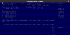
Thank you. This is a wealth of information! I did notice that there seemed to be two blocks of code, but I didn't know what to make of it. You explained it. I was looking at the code you identify as Test 2, which MattisLind pointed out as the subroutine at 3776, last night. It looks like location 2064 starts with the octal value 10 and then increments for the various related errors in Test 2. Plenty to analyze here and I am more confident now that we have enough information to get it back in working order. We seem to be focusing on a memory problem. I first want to compare board images thanks to czunit.
 
I think the DECNA memory is "real" memory and is mapped for general use. From what I saw in a technical document the issue was a stock Pro/350 with 512k of memory doesn't have enough to run the Decnet stuff, so they made sure you would with a bit of memory.

However it's possible that they wanted to use more space than the IO page for stuff, so did a Vax thing and blocked off 1/4 of the memory.

Anyway I took a few pics before jetting off here. These are low res versions, will upload better ones later. However I think the label is the MAC address, and mine does NOT have any wirework.

Let me know if there's a diff between mine and yours.

C
Thank you! This is very helpful. I need to study in detail later today, but at first glance it appears you and I have same variation board ("C1"), which means it has the same alternate part numbers for the memory chips. Manufacturing date seems to be close also. I did spot the wirework loop on the back in the same location. I missed it myself several times when looking at the real board. Your low res images are better than mine. I need to snap a few better images.

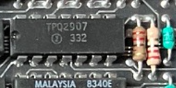
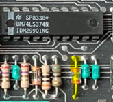
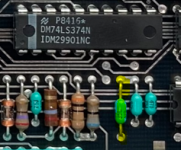
Well, later came sooner than expected. I visually compared the boards column by column looking at chip numbers and traces. The traces were identical back and front. There were some manufacturer differences in LS logic chip, just a few. The most significant physical differences are highlighted below. There are a couple of house marked chips on my board. A couple of capacitors are physically different. I assume that glass lined device is also a capacitor and there is one chip marked upside down. But it looks to have the right pin orientation. Otherwise, I would say they are identical.

1713277357624.png1713277466059.png 1713277498651.png1713277531795.png1713277606261.png1713277638508.png
 
Last edited:
I've done some work with the DECNA boards (I wrote a DECNA emulator for an Xhomer fork that more or less works -- it even booted disklessly). So I had to do a bunch of

That sounds interesting. How do you request a PRO to boot from the network?
 
Back
Top