• Please review our updated Terms and Rules here

VECTREX WITH PROBLEMS

They are the two small metal cans just near the video connector on the power board. One is Q401 and the other is Q402...

Only just got back myself - so I am just going to vegetate in front of the TV this evening I am afraid...

The information you need is in the Vertex Service Manual. Ok, it is not quite up-to-date with the specific version you have - but it is close enough to be very useful.

Dave
 

Attachments

  • Screenshot 2022-03-16 at 20.16.40.png
    Screenshot 2022-03-16 at 20.16.40.png
    66.6 KB · Views: 3
If you look back at post #256 I stated the diodes and transistor it could be.

Incidentally, I didn’t state to replace anything.

There are two ‘sides’ to the power board - the X side and the Y side. One of the transistors is in the X side and the other transistor is in the Y side.

We believe that the Y side is working. If this is the case, you shouldn’t be changing anything on the Y side...

Let me have a think and I will post some more investigation work for you tomorrow. I still don’t believe that twiddling the X SIZE potentiometer has no effect on the voltages we are reading on the connector. It should have. However, this effect may be relatively small and you may not have noticed it.

Dave
 
Good evening Dave, maybe can i try desolding Q401 to test with multimeter?
 
The first thing is to look at transistor Q401.

1647547080359.png

Unlike a 'normal' transistor, these devices should have four (4) wires attached to them (according to the schematic at least). A gate (G), source (S), drain (D) and the metal can of the transistor connected to GND.

Is it possible that one of the other three (3) leads of the transistor is in contact with the metal can of the transistor (or the GND wire)?

Dave
 
The first thing is to look at transistor Q401.

View attachment 1239445

Unlike a 'normal' transistor, these devices should have four (4) wires attached to them (according to the schematic at least). A gate (G), source (S), drain (D) and the metal can of the transistor connected to GND.

Is it possible that one of the other three (3) leads of the transistor is in contact with the metal can of the transistor (or the GND wire)?

Dave
Hi Dave, the Q401 and Q402 wires seems to be ok!
 

Attachments

  • Schermata 2022-03-17 alle 21.15.33.jpg
    Schermata 2022-03-17 alle 21.15.33.jpg
    153.5 KB · Views: 4
I have the next text procedure for you.

I just need to grab the computer with the real keyboard on it after my wife has finished her work for the day.

Dave
 
I have the next text procedure for you.

I just need to grab the computer with the real keyboard on it after my wife has finished her work for the day.

Dave
Hi Dave, thanks so much!
In the meantime must i resold power board or not??
Thanks again my friend ;)
 
A bit of information about what we are going to do:

1. These measurements are to be performed with the power OFF.
2. These measurements are to be performed on the Power Board.
3. I am hoping that the schematic I have matches your power board...
4. We are going to perform resistance measurements (using a multimeter) between 0V/GND and a specified point on the power board.
5. As we have a working channel (the Y side) and a non working channel (the X side) we are going to undertake resistance measurements and compare/contrast the readings from the X and Y sides of the circuit.

First of all, disconnect connector J402 from the power board. We don't want the logic board from affecting our readings. This is the connector with the RED and BLUE leads.

Second, select a suitable range on your multimeter to be able to read resistance values in the kOhm range. Connect the negative (black) lead of the multimeter to 0V/GND.

Set potentiometers R401 (X SIZE) and R408 (Y SIZE) to approximately mid scale. This step is important...

With the positive (red) lead of your multimeter, take resistance readings at the following points. Note that we will be measuring on ALL pins of each identified component (3 for the potentiometers and two for the resistors and capacitors). It is important to perform the measurements (and report the results) in the order I have specified the components. I will be 'switching' from the X to the Y side for each component.

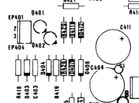
If you can't identify the component from the PCB silk screen itself you MUST consult the power board assembly drawing in the service manual (https://console5.com/techwiki/images/a/a7/Vectrex-Service_Manual.pdf page 14) to locate the component itself. The component identification may be on the PCB silk screen underneath the fitted component - so you can't see it!

The three pins of potentiometer R401 and the three pins of potentiometer R408.

The two ends of resistors R416 and R415.

The two ends of resistors R423 and R424.

The two ends of resistors R425 and R426.

The two ends of resistors R428 and R429.

The two ends of resistors R418 and R419.

The two ends of resistors R420 and R421.

The two ends of resistors R402 and R409.

The two ends of capacitor C403.

Some of these readings are duplicated - and will act as 'check' readings' for me to (hopefully) detect mistakes in the readings.

I will then print the schematic out and (using your readings) see if they make (a) logical sense and (b) if they point us at a faulty component (or permit us to 'zoom in' closer on a particular area).

Dave
 
Nice job! Ok now i'll start the measurement...
At the moment logic board is disconnected from power board.
 
So, under pcb:

R401 LEFT PIN= 1,417 KOHM
R401 RIGHT PIN= 3,25 KOHM
R401 CENTRAL PIN= 2,26 KOHM

R408 LEFT= 3,16 KOHM
R408 RIGHT= 1,425 KOHM
R408 CENTRAL= 2,24 KOHM

R416
PIN1= 1,413 KOHM
PIN2= 0

R415
PIN1= 1,425 KOHM
PIN2= 0

R423
PIN1= 2,26 KOHM
PIN2= 3,31 KOHM

R424
PIN1= 2,24 KOHM
PIN2= 3,31 KOHM

R425
PIN1= 7,84 KOHM
PIN2= 0

R426
PIN1= 7,75 KOHM
PIN2= 0

R428
PIN1= 4,80 KOHM
PIN2= 0

R429
PIN1= 4,65 KOHM
PIN2= 0

R418
PIN1= 3,31 KOHM
PIN2= 0,700 MOHM (the value start from 0,500 MegaOhm and after rises slowly )

R419
PIN1= 3,30 KOHM
PIN2= 0,700 MOHM (the value start from 0,500 MegaOhm and after rises slowly )

R420
PIN1= 3,31 KOHM
PIN2= 3,42 KOHM

R421
PIN1= 3,32 KOHM
PIN2= 3,42 KOHM

R402
PIN1= 3,42 KOHM
PIN2= 2,80 KOHM

R409
PIN1= 3,42 KOHM
PIN2= 2,80 KOHM

C403
PIN1= 91 KOHM
PIN2= 0
 
Excellent.

It is getting late here - so it must be an hour later in Italy...

I will have a look at the results tomorrow morning.

On a first look they appear to be consistent between the X and Y sides though.

Have a good night.

Dave
 
Excellent.

It is getting late here - so it must be an hour later in Italy...

I will have a look at the results tomorrow morning.

On a first look they appear to be consistent between the X and Y sides though.

Have a good night.

Dave
Yes "see" you tomorrow! Thanks and Goodnight!
 
Good saturday Sir Dave,
i saw that there is IC401 hidden under a big cooler...can be this bad??
 
You do like to guess don’t you? Unless you can find a cause and effect between IC401 and the observed fault you should not get distracted...

My best hypothesis would be a faulty IC306 (MC34001) assuming it is this IC that drives the X direction of the monitor (the signal on our blue cable).

My best hypothesis would be that this IC is not capable of driving any current into a load. This means that the output (from pin 6) will be OK without the cable connected to the power board. But, when we plug the cable in between the logic and power boards and add a bit of load resistance, the IC can’t drive the requisite output current and the output voltage collapses.

I have two tests that we can perform to prove my hypothesis, but I do know you like to replace components...

There is no 100% guarantee that IC306 is really faulty of course (this is why I would recommend performing some simple tests first). But, that’s up to you...

Dave
Dave i'm ready for your tests!
So...can i
now I have everything disconnected ... can I reassemble the boards and resolder the wires before to start with test?
 
First off - why am I discounting a fault on the power board?

Well, the 'front end' of the power board signal path pretty much contains passive resistors until we get to a little network of diodes.

R401 and R406 provide a fixed resistance of 2k + 1.5k = 3.5k between the X signal and 0V; whilst R423 (1.5k) is in series with any circuitry which follows the passives on the power board.

Let's assume a complete short circuit to ground after R423 shall we? This will result in a parallel resistance network of 3.5k and 1.5k leading to an effective resistance of 1.05k (to ground). at 5V, this would result in a current flow of 5/1.05 [mA] from the opamp. Let's call it 5 mA shall we. Technically, the MC34001 should only really supply 1.7 mA (max) so a direct short circuit could cause us an issue.

However, measuring the resistances doesn't come close to this value.

You were measuring 3.3k on the far side of R423 to 0V - leading to a current flow of 5/3.3 [mA] = 1.5 mA - just within specification.

Even if one (or more) of the diodes (D405, D406, D409 or D410) had gone short circuit, there are two further resistors that would limit the current flow - R425 (10k) and R428 (4.7k).

Therefore, it is unlikely that an active component fault within the diodes, transistor or power amplifier stages of the power board could realistically result in a current consumption from IC305 (on the logic board) enough to cause it to shutdown and significantly reduce the output voltage.

This is my thinking at any rate...

Dave
 
Last edited:
My tests are going to revolve around J402 on the power board. Please read my post thoroughly first to make sure you clearly understand what to do. If not, please ask further questions before performing the test.

Test the Vectrex again (after you have reassembled it) and make sure it is not working correctly again (it should not be working because we have not fixed anything yet of course)!

Draw out the connections on a piece of paper for J402.

There are two cables - one BLUE (X) and the other RED (Y).

Each cable is actually a piece of screened cable consisting of a signal core and an outer screen - both contained within the coloured plastic.

The outer screens of each cable are connected to 0V via connector J402 on the power board. It is easy to identify these two pins by measuring the resistance of all four pins of J402 to 0V (with the power off using your multimeter). The two metal pins that exhibit a very low resistance are connected to 0V. Mark these two pins with a red cross on your piece of paper. We do not want to connect anything to these two pins.

The remaining two pins of J402 are the signal pins. Mark the one closest to the blue wire as BLUE-X and the one closest to the red wired as RED-Y.

Disconnect the cable from J402 (if it is not already disconnected)

You have the MALE PINS of connector J402 on the power board and the FEMALE PINS of J402 on the connector attached to the red and blue wires.

The first test involves connecting the BLUE-X connection of the FEMALE PINS of J402 (on the end of the red and blue wires attached to the logic board) to 0V via a resistor of approximately 3.3k.

With the Vectrex running the diagnostic cartridge (you will not be able to see anything on the screen of course because we have J402 disconnected) measure the signal outputs from IC304 pin 6 (Y) and IC306 pin 6 (X) with J402 disconnected and the resistor NOT in circuit. Note the Vmin and Vmax voltage levels on your oscilloscope.

Then, insert the 3.3k resistor to 0V on the female pin end of J402 and observe the IC304/IC306 pin 6 signals again. Use your drawing on the piece of paper to guide you as to which of the four pins to attach to the resistor. Look for any discrepancy between the Vmin and Vmax voltages with the resistor connected verses the previous ones with the resistor not connected.

If you don't see any discrepancy, replace the 3.3k resistor with a 2.2k resistor and repeat the test.

I am hoping that the output from IC306 pin 6 (BLUE-X) will limit.

Try this test first and then we will see what the results are and (maybe) try my further test.

Dave
 
The first test involves connecting the BLUE-X connection of the FEMALE PINS of J402 (on the end of the red and blue wires attached to the logic board) to 0V via a resistor of approximately 3.3k.
Ok Dave but i connect to 0v of power or logic board?
Unfortunately now i can't find 3,3 Kohm resistor damn :(
 
Back
Top