• Please review our updated Terms and Rules here

CBM/PET 8032 not booting

Nope, you don’t need to change anything in the ROM.

Did you download my manual and read it? If in doubt, read the manual...

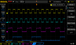
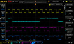
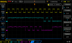
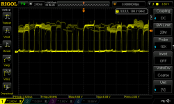
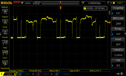
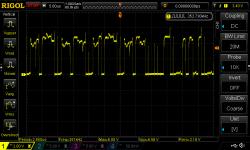
It looks like every other character is formed correctly. This could imply there is a fault with either the ODD or EVEN side of the video RAM.

I do see the odd German characters with umlauts, but some of the individual characters look like Romulan - implying the character generator ROM socket is not making good contact with pins of the ROM or the character generator is partially faulty.

My PETTESTER stores the characters sequentially from $00 to $FF into the video RAM, so if you check the Commodore PET documentation for the German character set you may be able to see some patterns forming.

Is that a ‘bespoke’ character generator I see on the board?

Dave
 
Hello Dave, thanks for the quick reply

I stopped before VDU test to make sure that I have burned the ROM correctly.

I've reseated the character rom (UA3) and tried to adjust the screen pots now. Unfortunately I don't have plastic screwdrivers so I have to guess it while the computer is off.

Here is a video with clearer results:

As you can see, every other character is flickery but the characters themselves look ok. Interestingly, the short section of PETSCII characters are stable except for the 3rd, 4th and 5th iteration.

Could it be the EVEN RAM then?

What do you mean by bespoke character generator? the F32 SC ROM? The other currently unused ROMs in the picture are just on a foam pad and included for reference. The board looks pretty original apart from the special ROMs.
 
UA3 is the character generator. I was just commenting on the fact that it wasn’t a ‘standard’ Commodore ROM, but had a hand-made label on it identified as “F32 SC”.

It was good for you to post a video explaining that the characters were changing. That accounts for the strange Romulan characters I was seeing! The photograph had probably ‘merged’ a couple of characters during the exposure.

On the fixed photograph I see the characters 0, 2, 4, 6, etc. interposed with random characters. The counting starts at the left hand edge of the screen with column 0. So the RAM circuitry to look at is the ODD bank.

I would suggest first having a look at the signals around UB8 (74LS373). This is the ODD video RAM data latch. You are looking for static signals, or voltage levels that aren’t true TTL values > 0.8V and < 4.5V. The upper voltage I have specified is not the true logic ‘1’ level, but this I would consider to be the practical limit.

If you have a TTL logic probe, it may be easier to just run around all the pins and reporting high, low, pulse or open depending upon the indicated state for each pin.

This test may not reveal the true fault however. I have a different test if it doesn’t!

Dave
 
As a side note but maybe important, I noticed that all the RAM appear socketed which is not the stock configuration. Was that done by yourself ?
I know from experience with that board it is easy to break a track or lift a pad…..worth checking all tracks are good


Andy
 
Last edited:
UA3 is the character generator. I was just commenting on the fact that it wasn’t a ‘standard’ Commodore ROM, but had a hand-made label on it identified as “F32 SC”.
Ok, as it's my first and only PET I have no idea what is custom or standard. So it probably would be good to have a backup of the ROMs with the orange labels.

It was good for you to post a video explaining that the characters were changing. That accounts for the strange Romulan characters I was seeing! The photograph had probably ‘merged’ a couple of characters during the exposure.

On the fixed photograph I see the characters 0, 2, 4, 6, etc. interposed with random characters. The counting starts at the left hand edge of the screen with column 0. So the RAM circuitry to look at is the ODD bank.

I would suggest first having a look at the signals around UB8 (74LS373). This is the ODD video RAM data latch. You are looking for static signals, or voltage levels that aren’t true TTL values > 0.8V and < 4.5V. The upper voltage I have specified is not the true logic ‘1’ level, but this I would consider to be the practical limit.

If you have a TTL logic probe, it may be easier to just run around all the pins and reporting high, low, pulse or open depending upon the indicated state for each pin.

This test may not reveal the true fault however. I have a different test if it doesn’t!

Dave

Fortunately no Romulans inside the machine :)

I'm not sure how to judge the signals, however everything was pulsing except Pin 3, which stays high. Oscilloscope pictures attached for reference (pin 20 got lost, but it's VCC anyway..)


As a side note but maybe important, I noticed that all the RAM appear socketed which is not the stock configuration. Was that done by yourself ?
I know from experience with that board it is easy to break a track or lift a pad…..worth checking all tracks are good


Andy

Yes, I socketed the RAM while waiting for parts (thought I might as well do it next to cleaning the board and replacing the caps). I tried to be very careful not to damage anything and inspected the traces before soldering on sockets. Time will tell if I missed something, the board is indeed delicate!
 

Attachments

  • ub8.zip
    1,007.7 KB · Views: 2
I haven’t looked at the ZIP file yet, but can I suggest a more ‘logical’ test solution with your oscilloscope?

Monitor UB8 (ODD video latch 74LS373) pin 1 (/output enable). I would suggest using this as a trigger for your oscilloscope.

When UB8 pin 1 is LOW, what are the output pins from UB8 indicating? More importantly, are some of them stuck high or low or are they toggling?

Perhaps read up on the terrible manual...

Dave
 
Hi Dave

None of them are stuck, they're all toggling. Q1 looks different (light blue trace). Might be due to D1 staying high, but I don't know if this is normal nor not.

ub8 q1-3 (1).png

The manual, while clear (and not terrible), doesn't help me because it assumes that the one reading it knows how PET video circuitry works (which I don't).

If there's a website, book etc. on how the PET internals work I'll gladly do some reading.
 
Sorry, I was referring to the oscilloscope manual, not the PET manual!

There are a few ‘old’ books available (now in downloadable PDF format) that do describe the PET circuitry. I can’t think of their titles just off-hand though.

When the yellow trace is LOW (the ODD video character latch enable) I only ever see the cyan trace HIGH. I would be expecting to see both HIGH and LOW signals.

I am not sure what I am seeing on the other two traces though (magenta and blue).

I am trying to work out whether it is the latch, the video RAM or the buffers that are faulty...

Just out of interest, are the video RAMs in sockets? Please say yes...

Dave
 
My scope is pretty self explanatory, no need for a manual... you're probably referring to the other thread with the 4016 PET (I sometimes look there to see if my problems could be related).

Magenta and blue are Q2 and Q3, they do have high and low signals as have all other ouputs except Q1. Sorry, should have included a picture of single shot mode, you can check the attachments (yellow is always /OE).

How does the logic on D1 / OSD0 (and others) work?

The video RAMs are not socketed.. but they can be... I also have a CBM 8050 disk drive that came with the PET, which looks like a nice organ donor.
 

Attachments

  • ub8 q1-3 (2).png
    ub8 q1-3 (2).png
    48 KB · Views: 4
  • ub8 q4-6 (4).png
    ub8 q4-6 (4).png
    49.9 KB · Views: 3
  • ub8 q7-8 (6).png
    ub8 q7-8 (6).png
    44.5 KB · Views: 3
Basically, you have ODD and EVEN video RAM.

Both sets of video RAM chips are latched into their respective latches at the same time.

Next, the EVEN latch data is presented to the character generator for one character time, followed by the ODD address latch.

This means that the Q output bus (to the character generator) will either see the EVEN latch data or the ODD latch data.

On the D (input) side of the latches you would generally have the data from the video RAMs to be latched. However, a CPU write to (or read from) the video RAM will cause the video RAM address and data bus to be ‘taken over’ by the CPU.

Note that the CPU reads (or writes) on one half of the clock cycle and the video circuitry uses the other half of the clock cycle.

Because the EVEN side of the screen is fine (what appears to be the correct characters - and they are stable) this must mean that the bulk of the video logic is fine. This means the problem must be somewhere on here http://www.zimmers.net/anonftp/pub/cbm/schematics/computers/pet/8032/8032029-09.gif.

The SAx and BDx busses are shared with the EVEN video RAM, so they must be fine.

The only signals that are unique to the ODD side are:

/CLK1B
/READ ODD
/WRITE ODD

I would suggest comparing the signals on the working (EVEN) side with the non-working (ODD) side to see if anything untoward jumps out at you.
You could possibly have some noise getting latched, or you could have a slow responding device or a number of factors.

Dave
 
Alright, many thanks for the explanation!

I probed the video RAM part, but could not find any obvious differences. When you mention noise, how would that look like?

While probing the data bus D0-D7 I noticed that the signals look "uglier" than others (see some samples attached).

That's where a working PET would have come in handy, because I don't have anything to compare to.

If anyone following this could be so kind and verify that this is normal, or even post some signals to compare?
 

Attachments

  • databus (3).png
    databus (3).png
    66 KB · Views: 5
  • databus (2).png
    databus (2).png
    42.9 KB · Views: 5
  • databus (1).png
    databus (1).png
    48.3 KB · Views: 5
Unfortunately, I think the databus is fine - as any issue will equally affect the ODD and EVEN video RAM signals.

The video RAM is generally decoupled from the CPU databus.

Dave
 
Ok, makes sense, just wanted to be sure. I had another look at the signals you mentioned on schematic 8032029-09. I missed it before, there is activity on BD0 but OSD0 is always high.

I will replace UB6, the 74LS244 in the next few days as I don't have any of those in stock.

Thanks Dave and have a good start of the week. Update will follow.
 
Basically, you have ODD and EVEN video RAM.
.....

Because the EVEN side of the screen is fine (what appears to be the correct characters - and they are stable) this must mean that the bulk of the video logic is fine. This means the problem must be somewhere on here http://www.zimmers.net/anonftp/pub/cbm/schematics/computers/pet/8032/8032029-09.gif.

The SAx and BDx busses are shared with the EVEN video RAM, so they must be fine.

The only signals that are unique to the ODD side are:

/CLK1B
/READ ODD
/WRITE ODD

I would suggest comparing the signals on the working (EVEN) side with the non-working (ODD) side to see if anything untoward jumps out at you.
Excellent analysis. I'd also like to see /READ Even and /WRITE Even compared to these signals. Looks like there is a typo on sheet 8. F8 pin 1 should be CLK1 not grounded.
 
There are a few ‘old’ books available (now in downloadable PDF format) that do describe the PET circuitry. I can’t think of their titles just off-hand though.


Dave
Dave,
If you can recall the titles of any of these books later, please post them. (I have been working my way through repairs on a spare dynamic PET board, which had a number of faults too). I would be interested to read the books.
 
Excellent analysis. I'd also like to see /READ Even and /WRITE Even compared to these signals. Looks like there is a typo on sheet 8. F8 pin 1 should be CLK1 not grounded.
Hello, I'm back.

Excellent.. and totally wrong. I noticed that some data lines on the video RAM circuitry were permanently high or low and it matched with the counterpart of the even side.

So I probed around some more before I would replace UB6 to see if there's more to it, and there was!

The reference to trigger off was the clock signal (as triggering off the signal itself won't tell you much in relation to what else is going on), in my case CLK1B(?) hooked up to UB8 (magenta trace).

Four signals looked different: OSD 4, 5, 6 and 7 (yellow trace), compared to the others (cyan trace):

DS1Z_QuickPrint4.png

My scope is bugging out here (on the number that mattered the most...), but the average pulses were six for normally operating data lines (all on the even side, OSD1-3 on the ODD side and four for the faulty part.

This narrowed it down to UC7 and UB7. Since I managed to obtain a replacement 2114 and 74LS244, I piggybacked both ICs to check for differences, and only piggybacking the RAM made one.

I went for it and;

20220510_001608.jpg

The CRT took too long to display the video RAM test, but I guess this is the next stage.

Find out more tomorrow when I put all the pulled chips back in to see where the result of the further tests.

It's gotten late and I have work tomorrow...
 
Dave,
If you can recall the titles of any of these books later, please post them. (I have been working my way through repairs on a spare dynamic PET board, which had a number of faults too). I would be interested to read the books.

Hugo,

The PET Revealed is one I can remember. I posted an online PDF reference to it in another PET thread. They are all merging into one now! I have so many PET threads on the go concurrently!

Dave
 
It looks like you are on to the page 0/1 memory test now with any luck. You may have fixed the video problem...

Dave
 
Hugo,

The PET Revealed is one I can remember. I posted an online PDF reference to it in another PET thread. They are all merging into one now! I have so many PET threads on the go concurrently!

Dave
Thanks Dave I found a link:


But I always seem to do better with a real book in my hand, so I bought this book on Amazon.

( Can never have too many books right ? One rare book I had on electricity and the principles of coupled tuned circuits, published in 1930, helped me with the analysis of the LOPT's in the PET VDU's)

Hugo.
 
Back
Top