• Please review our updated Terms and Rules here

Commodore CBM 2001-16N - BIG MESS!

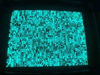
Hi Dave, Looks like you pointed me in the right direction! I just installed a new Character EPROM burned with the software you advised. I have done this exercise before when the graphic board was still installed and with a bad result. This time it is obviously improving. The screen picture is different with more randomness after each power cycle. A few times I could see some changes ongoing on the screen. I am getting somewhere....:)

I have checked Pin 10 on the video RAM chip F8 and it stays high. And yes, I already tried to replace the Video RAM but with the new RAM I get less different characters on the screen - a lot of @ characters almost everywhere. That's shown in my initial post. I still get the same result when using this other RAM. I guess it does not fit or is bad?

Now I still have the original 2114 RAM installed and both chips are getting hot over time! I think I have to look for a replacement.

Thank you!
 
And yes, I already tried to replace the Video RAM but with the new RAM I get less different characters on the screen - a lot of @ characters almost everywhere.

That may be progress. When the CPU comes up, it will clear memory. If you are getting a lot of '@' characters on the screen where you should be getting 'space' characters, it may mean the RAM is trying to work, but you have a problem with the signal SD5. Check then to see if it is being held low (ground) by another signal shorting it. It could also mean that bit 5 of the RAM is bad or a bad socket on F7. Note that a space character in RAM contains hex 20 (0010 0000). Screen Data bit 5 is set.
 
it may mean the RAM is trying to work, but you have a problem with the signal SD5. Check then to see if it is being held low (ground) by another signal shorting it. It could also mean that bit 5 of the RAM is bad or a bad socket on F7. Note that a space character in RAM contains hex 20 (0010 0000). Screen Data bit 5 is set.

Indeed, i found SD5 (Pin 13) on F8 is held low. How did you know? :) SD5 on F7 is pulsing!
All the other Pins of F7 and F8 look normal to me: 8/9 = Low / 10, 18 = High / all the others with PULSE
 
Indeed, i found SD5 (Pin 13) on F8 is held low. How did you know? :) SD5 on F7 is pulsing!
All the other Pins of F7 and F8 look normal to me: 8/9 = Low / 10, 18 = High / all the others with PULSE

Are you using the scope or the logic probe? F8-pin13 is signal SD1 and should be low most of the time. Remove F8 and see if ground is still there. Also F7-pin 13 (SD5) should be mostly high. Let's hope we are on the right trail.
 
Currently i am using my logic probe. Although i got now this analog scope it is more handy. I dont have a permanent repair desk at home therefore the big scope is stored away until i have more time for troubleshooting like on weekends.

I briefly checked again today. Yes, the Video Ram at F8, Pin 13 (SD01) is mostly low - only few times it is showing high.
While checking i noticed something. When i push on F7 with my finger the character pattern on the screen is changing (better to say alternating). So, although i already installed sockets on F7, F8 there might be a bad contact somewhere. Will check on the weekend...
 
I'd like to suggest an experiment. I'm not sure that the video RAM is being written to. I'd like to confirm the address decoding to the video RAM.
With the NOP generator in place we can do some checks, with the scope.
First set channel 1 as trigger source for positive edge.
Connect to B3 pin 9 ( BA15 )
Adjust sweep for the positive level to be 16 horizontal marks wide ( you 'll need to adjust the center knob of the horizontal sweep ).
With the vertical channel 2, probe F5 pin 13.
You should see a positive pulse for 1/2 of a division at the beginning of the positive pulse on channel 1
This would indicate that the address decoder is working correctly. Anything else would mean there is a decoder problem from the processor.
Continue with channel 2 and measure F5 pin 8. This should be the inverse of the one seen at F5 pin 13.
Let us know what you get and we can go from there.
Dwight
 
I'm likely looking at the wrong schematic. I get confused when looking for these.
Its late, I'll look in the morning to see what I screwed up. BA4 wasn't what I was expecting.
Dwight
 
I'd like to suggest an experiment. I'm not sure that the video RAM is being written to. I'd like to confirm the address decoding to the video RAM.
With the NOP generator in place we can do some checks, with the scope.
First set channel 1 as trigger source for positive edge.
Connect to B3 pin 9 ( BA15 )
Adjust sweep for the positive level to be 16 horizontal marks wide ( you 'll need to adjust the center knob of the horizontal sweep ).
With the vertical channel 2, probe F5 pin 13.
You should see a positive pulse for 1/2 of a division at the beginning of the positive pulse on channel 1
This would indicate that the address decoder is working correctly. Anything else would mean there is a decoder problem from the processor.
Continue with channel 2 and measure F5 pin 8. This should be the inverse of the one seen at F5 pin 13.
Let us know what you get and we can go from there.
Dwight

Change F5 to A5. It should be A5 pin 8 and A5 pin 13.
Ok back to sleep.
Dwight
 
Hi Dwight,

i agree with you, the Video RAM is still not being written to.

Yesterday i received my new Video RAM. After installing i get different characters on the screen as with the original RAM but the pattern looks quiet similiar. From my point of view there is no improvement.
If i put RAM chip #1 in the F7 socket and #2 in the F8 socket it looks different then when i put #1 in F8 and #2 in F7. Just different characters on the same spot. What is funny - when i change back -#1 in F7, #2 in F8 - i get the same characters on the screen as initially. Like each individual RAM chip is storing it own characters as shown on the screen.

The bad contact was on the socket F7 which i was able to solve with some de- oxid.

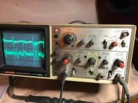
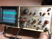
Today i did the „experiment“ as you suggested. I tried to set up my scope according your instructions (still learning how to handle the equipment).
Unfortunately i was not able to sweep 16 marks wide – i only have 10 „squares“ on my screen.
I also did not understand what „i should see“. I need to get used of the „scope language“:confused:

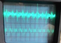
I did make photos of the results. Is this telling you something?

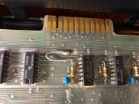
Some interesting thing i found. There is a jumper wire from Ground to Pin 9 of A5. Not sure what it effects. I did cut this wire and measured one more time. See attached photo.

Have a nice sunday :D

Garbage Screen NEW RAM 9.5.20.jpg
Scope CH1_B3-9_CH2_A5-8.jpg
Scope CH1_B3-9_CH2_A5-13.jpg
Scope CH1_B3-9_CH2_A5-13(Jumper cut).jpg
A5 Jumper mod.jpg
 
Denis,
Set trigger control to 'normal'. Set vertical inputs to .2 V if you are using a 10X probe or to 2V is using a 1X probe. All we are seeing right now is noise.
 
Denis,
Set trigger control to 'normal'. Set vertical inputs to .2 V if you are using a 10X probe or to 2V is using a 1X probe. All we are seeing right now is noise.
... and make sure you have a good ground.

I'd pull that jumper a5-9 to ground; looks like it should be high to load the RAM.

Also it looks like some corrosion around there; wouldn't hurt to clean it up a bit.

Finally, the persistent vertical line in the second-last column might point at the character generator chip; check all the pins there.
 
Thanks for sending a picture of the scope. Thanks Dave for helping on the setup. We ar looking for signals that would be on the order of 2.5 to 5Vn not some fractional volts.
You could use the width of the positive pulse as 8 ( power of 2 ). The reason I was looking at this is that the pulse we are looking for should only be 1/32 of the width of the A15 signal being high. It is qualified by A15, A14, A13, A12 and A11. I may have done my math wrong but it would be a short pulse.
I talked about the center knob but it is the knob called SWP VAR.
You also want to adjust the POSITION so that the sweep starts on the left of the scale on the sceen. You have it off to the left someplace??
The position knob also has a 10X mode. Do not use this for this experiment.
I like to put the chan 1 as the top trace and chan 2 as the bottom trace. I'm not at all sure how you have these arranged.
In the NORMAL trigger you have to have a signal there. That would be A15. It is a large slow square wave. You'll need to adjust the LEVEL knob using the NORM position.
It is going to be about 15 Hertz. Half a sweep for the screen width will be .1 or .2 seconds, not microseconds.
For the display MODE, CHOPPED will usually work better for slow signals, although ALTERNATE will also work for a repeated signal such as we have with the nop adapter in there but at such a slow sweep speed, it will be difficult to look at. An alternative with digital signals is to use ADD but analyzing the two signals together as a single trace can be confusing.
You may not be able to take a picture without a slow shutter speed camera.
Dwight
 
Thank you all for you friendly suggestions and corrections. This helps me a lot to understand how to use the scope and how to move on.

Indeed I measured noise. Now I know how it looks like:D

I soldered the Jumper back to A5-9 and I also tried to clean up the board with IPA in the mean time. However it did not improve that much. It stays a mess board.
I got good ground. I connect my probe to one of the GND pins at G9 which is very close to the point of measurement.
About the Character ROM F10 – I changed it already and could verify the software with my programmer. It´s a brand new EPROM installed now.

I did set up my scope to 2V yesterday (I do not use the 10x probe setting) and measured around 4V at B3-9. I took me a while to capture a signal. I am unable with the trigger to get a motionless wave on the screen. It is around 15 screen units times 10ms means 150ms, so ca. 7 Hz. That’s something what I would expect at A15, starting with 250 Khz at A00 (I understood the NOP takes 2 cycles, correct?).
I did struggle to capture the signals of A5-13 and A5-8.

I will try again later today or tomorrow with the new instructions from Dwight (I read after my measurements yesterday). I will likely filming the measurement with my Phone, so I can hopefully catch the square waves.

I also want to let you know that I did some further tests yesterday with my logic probe and without the NOP Adapter and want to share my results with you. On the CPU I found the Reset working properly and the Clock In Pulse (37) available. But no Pulse on Clock out (39) and but no High nor Low at R/W (34).
I found no Pulse at all on the address lines but that´s not a big surprise because the systems stucks somewhere as we know.
Maybe the status of the Data Lines is pointing somewhere? D0, D1, D3, D4 are Low and D2, D5, D6, D7 are High.

I found the 6522 (C4) and Kernel ROM (D9) is getting warm, the CPU is cold.

Please note, my posts with photos attached take sometimes before showing up here. Probably because I am a new member…
 
Sorry, in all this I missed that you'd removed and replaced the A5-9 jumper; is there a difference with it grounded or not? I think it should probably be disconnected.

Re the CG ROM: I was suggesting that you check the connections (IC pin to pin) between it and E11, especially pin 16 to 5, for continuity.

Do I understand correctly that you get activity on the address lines using the NOP gen but not in the normal configuration?

I did not see any difference yet when i cut that jumper. Its been soldered back now. I can cut again at any time.
About the CG ROM. I did not check all pin connections yet - will put this on my TO DO List.
And yes, with the NOP installed i get activity on all address lines at the CPU and i get pulsing signals on the majority RAM and ROM pins. Without the NOP Adapter and the CPU directly installed there is no Pulse on the ROM´s and RAM´s.
 
Back
Top