• Please review our updated Terms and Rules here

Commodore PET CBM 4016 ASSY 8032080 RIFA burn and more

DrAlis

Experienced Member
Joined
Nov 11, 2021
Messages
221
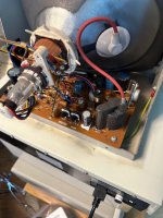
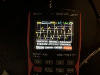
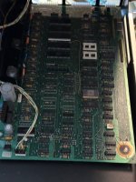
Dear all, in the process of trying to repair a PET, I had a smoke development and FI / RCD breaker tripping event. The suspected RIFA that burned was removed but the PET would still not run just like before. This was followed by a solder trace burnout on the back of the PCB (one of the power rails). I repaired the trace and suspected something wrong in the power supply. I also measured around the rectifiers and what not but came to no conclusion. So I went to try the bridged PCB in one of my working PETs (bad idea). Well, then I had a power supply smoke event with additional FI / RCD entertainment and damage to the previously working PET. Plus, I felt slightly sad and not so smart afterwards. Interestingly, despite the smoke and FI / RCD, the previously working PET is still working but has suspicious power draw even when off. And here are my questions for you experts:

  1. How much power usage is to be expected when the PET if off? (Mine now draws around 1W. I guess from the RIFA and that seems wrong.)
  2. Is it possible that a damaged mainboard destroys the RIFA?
  3. Any advise on how to continue my fixing procedure :)
  4. Why are almost all my PETs making this pretty loud humming sound when they are on? (Can it be ignored or is it a safety concern that needs fixing:)
Thank you all and happy easter
 
Just out of interest, what RIFA are you referring to in the PET?

Can you post a photograph of the damage?

To (partially) answer your questions:

1. Strange...

2. No.

3. We need to view what the damage was and where first.

4. Three possibilities:

4A. The transformer is overloaded due to a high current draw. This needs to be investigated.

4B. You have a 60 Hz computer running at 50 Hz.

4C. The transformer laminations are lose. This is ok. Try tightening the bolts up on the transformer a bit more (if there are any) to see if this reduces the problem.

Not a wise decision (I am afraid) to transplant a faulty board into another machine. The more likely possibilities are a short circuit bridge rectifier or diode CR3. These would (effectively) short circuit the transformer secondary.

Dave
 
Last edited:
Hi Dave, glad to see you again. Thanks for your feedback.

With RIFA I intended to refer to the RFI cap sitting inside the metal box next to the power socket. You are correct it is not the traditional RIFA brand.

I forgot to take the right pictures but will do and deliver tomorrow. Thanks.
 
The 'RIFA' capacitor(s) going are just 'expected bad luck'. It is very unlikely that any fault on the PET will cause these RFI filter capacitors to die.

In order to proceed, I need to know what died on the PET(s).

Dave
 
The trace burn happened on the bottom of the picture, above the middle of the gold connector. Putting the board under power seems unwise. So desolder one/both bridge rectifier or is it possible to measure them while in place?

IMG_8965.jpeg

As for the second PET board, it still works so no issue. For the (two) power supplies, I will disconnect the RFI caps. This should fix the power draw also, as they are the only things connected when the PET is switched off, correct? I heard smoldering sounds from the power block during one of the failed tests. Since the fuse did not blow, is it reasonable to assume that the actual transformer was not harmed, but the sounds likely came from the RFI?
 
Last edited:
So the 0V line from Q1 & Q2 up to connector J11 pin 7 has suffered an 'overload'. Either Q1 or Q2 have failed badly or something has made contact and shorted to 0V though this line.

Was there any contact between any part and the point of failure ?
 
Trace burns like that are nothing at all to do with Rifa capacitors failing.

They generally happen in cases where:

1) Tant capacitors or less commonly electrolytic short out and even less commonly 0.1uF bypass capacitors short, and combined with;

2) Inadequate current limiting on the power supply feeding the track.

In most cases because the power feeds come via analog voltage regulator devices (which have excellent overload protective systems -unless replaced by a switching regulator equivalent, or the board powered by an alternative power source than standard), the analog regulators virtually never cause this, because when overloaded they go into a low current shut-down mode. However, if the section of track that got cooked is prior to a voltage regulator, and say directly out of the rectifier system on the transformer secondary, it is another story.

So, if you can correlate the burnt up track with the schematic and explain if it is the standard power supply, or not, it will be very easy to explain what went wrong here and why the track got cooked up.

Don't expect the transformer's primary fuse to be of any help here. Lets say it is a 1A fuse, in a 110V system you can get 100W of heat before the fuse blows and in a 220V system twice that.

The purpose of the primary fuse is to protect the wiring on the transformer primary side, not pcb tracks or semiconductors on the secondary side of the transformer.
 
Last edited:
The burnt track is the Unregulated +9V rail to Q1 and Q2 feeding the cassette motors.

The usual issue here is either plugging a cassette drive in the wrong way around - or connecting something other than a cassette drive to one of the cassette drive ports.

There is very little else on the +9V UNREG rail that could case this. Even a short circuit Q1 or Q2 would not cause it if it was between the collector and the emitter.

When a cassette motor is switched on (sometimes at power up) there will be a very large current flowing from the unregulated +9V supply, through transistor Q1 or Q2 and to ground.

Did you have any peripherals connected at the time of the smoke signal or not?

The unregulated +9V is taken directly after the bridge rectifier and large external reservoir capacitor - but before the voltage regulators. Basically, there is absolutely no protection at all for these types of faults (by poor design)...

Dave
 
Thank you for the expert attendance. Proud to have Hugo & Gary here, too. Great insights on fuses, trace burns, transformer noise and tape drives already ;)

OK, so the RIFA/RFI deaths are likely unrelated by logic and consensus. No peripherals where connected at any time. Also, I am fairly confident no bonus conductors (like loose screws etc.) assisted in the short. Even thought the PCB was not screwed down tightly during the test, so there is a residual risk. The damaged trace comes from J8 Pin 2 (if Pin 7 is KEY Pin) as you correctly pointed out.

Any good ideas on how to proceed? Thank you.
 
Yes, J8/2 and it disappears off to J11 pins 1, 4 and 6 as well.

Take a close-up photograph of the damaged area itself. Unfortunately, you can't see too much detail when you blow the last photograph you posted up (no pun intended)...

Clean up the area and see what the damage actually is.

Before 'fixing' anything, I would suggest trying to find any direct short circuit (using a multimeter on a low resistance setting) to any other power rail. +9V shorted out to any other power rail (+5V, +12V, 0V or -5V) will do damage.

Check both sides of the damaged PCB track.

Also, check the immediate area for any other PCB tracking casualties.

Then we can look at the repair.

Dave
 
You can admire my terrible soldering skills below. I already fixed it. As per my story, I put it in the working PET with the somewhat scary outcome that turned out mild (no harm - maybe?). So no option to wait for bridging the burned trace. I did measure some resistances as follows:

J8/2 to
-5V: 9.8 MOhm
GND: 3.8 MOhm
+5V: 0.7 MOhm
+12V: 3.9 MOhm

Also used the 4116 RAMs to measure resistances on the board as follows.

GND to
-5V: 10 kOhm
GND: 0 Ohm
+5V: 352 Ohm
+12V: 7.9 kOhm

I also just realized that two of the standoffs where the PCB is held on in the case are METAL... I did not realize that fully as I am used to the plastic clippie standoffs.

So there is a chance that I fried it by not placing it perfectly straight and aligned on top of the holes on the standoffs while doing my testing. This could make me the cause of the trace burn by shorting something in close proximity of the holes and the board being dead for something unrelated such as RAM failure etc... So there is a chance there were three independent issues.


IMG_9471.jpeg
 
Last edited:
I would clean up all of that black 'mess' around the PCB track though.

Use a cotton bud (or 3) and Isopropyl alcohol.

It is interesting that there is apparent heat damage to BOTH sides of the PCB track - implying a high current has flowed BOTH WAYS. I didn't expect that...

Do you have access to a current-limited variable voltage bench power supply?

Dave
 
Thanks Dave, I will do the cleaning but that is only cosmetic, right?

I have an adjustable voltage power supply, but not one that limits currents unfortunately. But I guess I can buy that too now...

I have a osci-/multimeter and plan on comparing the J8 inputs of the two machines. Too bad part of the power supply is on the mainboard, so I guess I can only see the AC coming out of the transformer, right?

Your current flow direction observation puzzles me. Isn't it just getting hot and smoldering equally in all directions? What I find strange is why it burns there. Seems the trace gets narrower towards the bottom of the picture. So it should have higher resistance there and burn earlier?

I am also thinking about putting the working PET mainboard into the other case to see if monitor and power supply are working on the dead one. But I guess, I see more risks now and will hold off this experiment...
 
There may be suspended conductive pieces in the black - so not purely cosmetic.

We can also see more clearly the damage.

I would resist the temptation to swap boards!

I would ALWAYS disconnect the power supply connector from the main logic board and monitor and measure the AC secondary voltages from the transformer as normal business.

I would also check the earth bond resistance and electrical isolation as well for safety.

Dave
 
Parts of the track heated more than others, because of the thickness of the solder layer on it, where it is thicker the resistance is lower and where pins are soldered there is more thermal conduction away from the track. A fairly long length of track got uniformly heated and you can see the green coating over it changed color. Copper has a positive temperature coefficient so the hotter it gets the higher the resistance, so when the current is high enough (if the power supply can deliver it) and a zone of the copper gets very hot, it is a positive feedback like effect and that area will dissipate more heat and so on, and finally melt. Definitely a direct short caused this problem,
 
Thanks Hugo. So you say a direct short caused this. I measured resistances from the burned and fixed line to GND and all 3 Vs and all where in the MOhm range. So there is no short now. Is it fair to conclude that I caused the trace burn by bad placement of the PCB during the first tests (I shorted something with the two metal stands the pcb sat on unintentionally). On the positive side this means there is no short on the board and I can power up the board
closely monitoring temperatures with my thermal cam. before all that I check my AC voltages and earth resistances as per Dave...
 
Last edited:
I am getting convinced I caused the short at the bottom right hole of the pcb. the pcb was unscrewed and sat loosely on the plastic stands and the 2 metal stands. i did not realize that there were metal ones. if i just misaligned it by 2mm it could have shorted some of the 3 legs of the transistor / regulator q2 as per below zoom picture of the entire pcb. there is also discoloring residue.

IMG_9495.jpeg

assuming i only broke the trace, i could now move to other causes than the trace like ram etc.
 
Last edited:
My dear virtual friends, I report not victory but progress. Broken trace cleaned and fixed. Transformer voltages checked and both PETs compared and equally nice. Felt confident enough to put board back in after checking for shorts with multimeter. Powered up the board. Checked +5V and +12V while live and looked fine. Strangely unit only draws 50W (rather than 70W as my other unit). But no chirp and absolutely black screen no nothing. Opened monitor assembly. Dusted stuff off. Lots of of on and off switching of the unit. Suddenly: the famed GARBLED CHARACTER SCREEN appears. I rejoice. I never had it but read plenty about it. I guess now it is time to read it again. Then, screen goes black again. More power cycles. Now. I only get an ultrabright green dot in the center of the screen. I get disappointed something broke again. Quick cool down time of the unit. And then the garbled screeen is back. Sometimes the board even chirps, sometimes it doesn't chirp, sometimes it chirps in endless repeat. Well, I guess now I wish I had Dave`s PETTESTER... Which I don`t have yet. But I am pretty happy I got to see an image on the screen. I call this progress and we can work it from here. For joy I add some pictures below. Thank you all so far :)
 

Attachments

  • IMG_9535.jpeg
    IMG_9535.jpeg
    133.6 KB · Views: 10
  • IMG_9530.jpeg
    IMG_9530.jpeg
    1.8 MB · Views: 10
  • IMG_9526.jpeg
    IMG_9526.jpeg
    2 MB · Views: 8
  • IMG_9523.jpeg
    IMG_9523.jpeg
    1.6 MB · Views: 6
  • IMG_9513.jpeg
    IMG_9513.jpeg
    1.3 MB · Views: 6
  • IMG_9515.jpeg
    IMG_9515.jpeg
    3 MB · Views: 7
  • IMG_9528.jpeg
    IMG_9528.jpeg
    130.2 KB · Views: 6
Last edited:
You really need a copy of my PETTESTER...

Although the green spot in the middle of the screen is more likely to be the monitor.

The constant chirping could be a ROM, RAM or IC socket issue.

It could also be multiple resets.

There are too many unknowns at the moment and we need to convert unknowns into knowns...

Dave
 
Back
Top