• Please review our updated Terms and Rules here

Original-IBM-5150 or IBM-Clone Memory Experimentation Thread

I took a quick look at the circuit diagram in post #110, looking at just the circuitry that generates the lines you have marked as CAS0 and CAS1.
I can see that in the 640KB configuration (JP6 jumper in), the 256Kbit chips go into the two banks associated with the lines that you have marked as CAS0 and CAS1.

Taking a quick look elsewhere in the diagram, I spotted an error. See the red line at [here]. None of the connected pins is an output.
 
All right. I drug out the oscilloscope once more, just to see if the problem lay in the inputs and outputs. So far, no problem yet. I am getting data pulses on A8, but these pulses should be few and far between compared to A0-A7, correct? A0-A7 seem to be constantly busy.

(I know it seems like I'm randomly nitpicking and looking for a problem, but I want to make sure that any bases that can contribute to this memory working get covered.)

I sent off for my IC clip and cables yesterday, so I'll see if anything odd pops up when I test the logic next week.
 
Last edited:
All right, I got my stuff in. I'm not sure if I am doing the logic testing properly (I doubt it), so I might not follow on it, but I have followed on the lead of the bits 1, 3 and 5 failure. This guide on minuszerodegrees shows me the exact symptoms that I have with the board and the normal POST (without the diagnostic ROMS): https://minuszerodegrees.net/5160/ram/5160_ram_256_640.htm

The bad bits do not jump around with swapping the installed chips. My suspicions draws me closer to thinking this is a logic problem. I will check Port A on the 8255 tomorrow.
 
Last edited:
I am getting data pulses on A8, but these pulses should be few and far between compared to A0-A7, correct? A0-A7 seem to be constantly busy.
Keep in mind that if RAM refreshing is going on (as initiated by the motherboard's BIOS ROM, or by a diagnostic ROM), then the RAM refreshing mechanism will be 'running interference'.
For example, per [here], the IBM BIOS ROM on an IBM 5150 motherboard initiates RAM refreshing that uses the least significant 16 bits of the address bus (i.e. A0 to A15).

With the motherboard's BIOS ROM in place, IRQ 0 (for 'system timer') will be triggered at about 18.2 Hz, and each time that happens, it's a jump from wherever into ROM space.

The bad bits do not jump around with swapping the installed chips. My suspicions draws me closer to thinking this is a logic problem.
I agree.

Taking a quick look elsewhere in the diagram, I spotted an error. See the red line at [here]. None of the connected pins is an output.
Did you investigate that? (Circuit diagram error, or the board is actually erroneously wired that way?)
 
For the error in the diagram, I didn't check.

I did, however, check the pins on Port A of the 8255. They're all being pulled low. Shouldn't they be toggled?

Ruud's Diags still show bad bits 1, 3, and 5. However, it seems that the Supersoft Diags have changed. It shows ALL bad bits from 0-7. (Although this seemed to happen after I unplugged the floppy drives. I'll check later)

There is one oddity that I'm suspicious about... Should the diagnostics show 8255 Parity all the time, or is there something wrong? I do have an S280 parity generator installed, but with the Supersoft Diagnostics, parity still exists even without the S280.
 
Last edited:
I did, however, check the pins on Port A of the 8255. They're all being pulled low. Shouldn't they be toggled?
Did you mean "be drive high", or "be toggling" ?
And in either case, where did you get the information from ?

There is one oddity that I'm suspicious about... Should the diagnostics show 8255 Parity all the time, or is there something wrong? I do have an S280 parity generator installed, but with the Supersoft Diagnostics, parity still exists even without the S280.
No.

Refer to the IBM XT diagram at [here]. Your motherboard is expected to be similar. Parity errors are signalled (signalled by parity error detection circuitry) to the BIOS (or diagnostic) via two pins of the 8255. Before any RAM reads are done by the diagnostic (or BIOS for that matter), those two pins should be indicating no parity error occurred. The diagnostic saw otherwise.

1683962005551.png
 
Did you mean "be drive high", or "be toggling" ?
And in either case, where did you get the information from ?
I found them here:

I followed the steps until I got to step 6, and I didn't get any pulses out of the 8253.

Since none of the problems on the next relevant page of the diagnostic don't fit my situation (because it's affecting all the chips, and swapping doesn't change the problem), I skipped to Step 5:

Then I ended up on this page.

There is no activity on Port A pins of the 8255. Everything is logic LOW. (I even tested with an oscilloscope and a logic probe. No voltage on the oscilloscope, and the logic probe showed a low signal.) I believe I just happened to test it with the Supersoft Diagnostic, and it doesn't stop on an error, so there would be activity no matter what.

As for the schematic error, I can check it later. Before my suspicions about it being a logic problem, I was more concerned about whether the 256/640 circuitry actually existed on the board.
 
Last edited:
Then I ended up on this page.
You are using diagnostic procedures that target the IBM 5150/5155/5160.
Some parts are not generic.
It is wrong to assume that authors of motherboard BIOS' for clone computers copied everything that IBM put into their motherboard BIOS'
The 8255 port A behaviour in shown at [here] probably isn't in your BIOS.
 
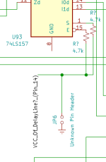
Something else in the circuit diagram is wrong. I picture the area below.

If a jumper is placed on JP6, it will short the Vcc pin of the delay line to ground !

I suspect that:
- Pin 15 (/enable) of U93 is grounded (as was mentioned in an earlier post).
- Pin 1 (select) of U93 goes to JP6, with there being a pull-up resistor on that line to the Vcc pin of the delay line.


1683968602855.png
 
The problem is when you have the board set to 640K configuration. You know from Ruud's diagnostic ROM that, in that configuration, there is a problem somewhere in the first 2 KB of addresses. Maybe all of them.

A way ahead is:
Step 1: Use an EPROM containing custom code to discover and report the first 'problem' address in the first 2 KB of addresses. Maybe the first is address 0, maybe not.
Step 2: Use an EPROM containing custom code to, in an endless loop, write and read the address discovered in step 1.
Step 3: Using a logic probe (or oscilloscope), look for some basics such as RAS and CAS pulses arriving at the applicable RAM chips (the bank that hosts the first 2 KB of addresses). And no RAS/CAS appearing at other banks.
Step 4: Using an oscilloscope or logic analyser, verify that there is a delay between RAS and CAS. (To be sure!)
Step 5: Using a logic probe (or oscilloscope), and referring to the circuit diagram, and using knowledge of how the circuit works when reading/writing RAM, look for anomalies.
Step 6: If required, step 5 but using a logic analyser.

The custom code would not initiate the RAM refresh mechanism. It should not need to - reading/writing is happening frequently enough. With no RAM refreshing going on in the background (and nothing else such as INT0), any RAS/CAS/address activity must be the result of the endless loop of writing and reading the first 'problem' address.
 
Would I be able to use the 5160's BIOS to get the bit error pattern on Port A?
You could give it a go. A question (rhetorical) though is, is the Sanyo MBC-775 close enough to the IBM 5160 for that to be valid. The other thing is, if valid for the Sanyo MBC-775, and multiple bits are involved, the port A byte will sometimes show only some of the bits (per the multi-bit discussion at the bottom of [here]).

And you are not going to be informed of the failure address, which could aid things. You know from using Ruud's diagnostic (in post #116), that the first-found failure address is somewhere in the first 2 KB - address 0 should not be assumed. In between other things, I am modifying Ruud's Diagnostic ROM, and a mod is to get the 'first 2 KB RAM test' to display the first found faulty address, and all of the bits-in-error at the address. That may help, particularly in regard to 'Step 1' in post #133.

But one thing you should investigate now is the failure of the '8255 PARITY' test of the Supersoft Diagnostic ROM, as discussed in the second half of post #126. A fault on your motherboard, or due to the MBC-775 not being close enough to the IBM 5160! What is going on there?
 
All right, I finally got things in order. I have a logic analyzer. Your version of Ruud's diagnostics shows a failure on the very first address that it reads: 0000 (I forget the format, but the point is that the diags reports a failure in memory right out of the gate, at address zero.)

Logic activity, at first glance, doesn't show anything out of the ordinary, according to my logic analyzer.
 
@modem7 : I'm going to go over the schematic you provided for the NMI and parity check, to see if I can add more to my own Sanyo schematic, and check the differences. I know there's a chip on it that does the same functions as the parity error reporting.
 
All right, I finally got things in order. I have a logic analyzer. Your version of Ruud's diagnostics shows a failure on the very first address that it reads: 0000 (I forget the format, but the point is that the diags reports a failure in memory right out of the gate, at address zero.)

Logic activity, at first glance, doesn't show anything out of the ordinary, according to my logic analyzer.
Later today, I will quickly knock up some code-for-ROM that will, in a loop:
1. Write 55h to address 0.
2. Delay.
3. Read from address 0.
4. Write AAh to address 0.
5. Delay.
6. Read from address 0.

I will put that into my IBM 5150, then do a capture on a bank 0 RAM chip using my logic analyser, then present that capture here.

( RAM refresh will not be set up. In this test scenario, it doesn't need to be. And with it off, the capture is 'cleaner' to view. )
 
Just to let you know, the logic activity I looked at was all the pins on one of the memory chips. It looked normal based on how it looked when the system read the memory as 64kbit. I don't know where to start with something like this.
 
Last edited:
Back
Top