• Please review our updated Terms and Rules here

Plugging in power to other side..

I am beginning to think that removing the 8080 CPU (thus exposing the address bus, data bus and control bus) and manually driving/monitoring these signals will help isolate the fault to a sub-section of the circuit.

Let me think a bit about this and see if I can come up with something relatively simply...

Dave
For sure. I have been checking every pin and socket but I just can't find whatever is doing this. It is consistently lighting every data LED on port 2. I've checked every trace near where I'm pressing down to make it work.. all look good even when not. Could be a bad contact anywhere. I'll be checking CPU and that area next.
 
Have you performed this test yet:

>>> I would next check pins 4 and 13 of the 7475 latches used for the address and data LEDs. I would expect to see short, high-going pulses to latch whatever is on the data bus into the latches. These latches become transparent (will pass through whatever is on the data bus to the LEDs) if the signal is HIGH.

These pins could be quite telling as to what is going on with the machine 'quiescent'. It should be reading from the keyboard port and not writing to the LEDs. As a result, all of these pins should be permanently LOW.

Dave
 
Well they shouldn't!

The firmware should be sat in a tight loop waiting for a key to be pressed and released. So the only activity should be on the input port.

Perhaps we should pursue this line of enquiry?

Dave
 
Well they shouldn't!

The firmware should be sat in a tight loop waiting for a key to be pressed and released. So the only activity should be on the input port.

Perhaps we should pursue this line of enquiry?

Dave
I think so. My challenge right now is, I can only make the firmware activate by physically bending the board gently at one place. It will not operate without that pressure applied. So I'm thinking I have to nail down what exactly is not getting connected. Unless what I'm actually doing by pressing down is 'breaking' a connection, and the machine was 'working' because it was partially broken somewhere. So many possibilities.
 
Ok.. slight mistake.

Quite a while back I had read in the manual that the machine could run on just two 8111 chips. So I installed just 2 for troubleshooting purposes, to simplify matters. However, I had them in the bottom two sockets (IC11 and IC12?) whereas the manual said they should be in the top two (IC9 and 10). Can't explain how it worked like that.. but with the two chips moved back to the top sockets.. it does not execute the PROM.. least as far as I can see.. it just fires up showing address 5 on the display and does nothing further. Also installing all four 8111 RAMs also freezes the machine. It only somewhat works if you have just 2 RAMs in IC 11 and 12.

I traced all the CPU pins on the schematic around, verifying it connected to memory lines in particular but also checking other pins. Followed DBIN through IC1, saw it get inverter through one gate, then inverted again. Looked alright.

Checked all the data pins from the CPU to IC6 and IC7, all the connections are good.

Then I moved up to IC13 and checked all the inverters. One inverter that stood put was pin 9 and 8. Pin 9 looks like a nice clean square wave, same as it looks on pin 39 of the CPU. I'll expected to see essentially the square wave on pin 9 to be an inversion of itself on pin 8.. but it looks different. Each power up usually made it look like my second picture attached (the first one with the thin little square wave is from pin 9), sometimes it looked more like a sine wave. I bent pin 8 out to see what was going on.. but nothing. Meanwhile, at the socket for that pin, something that looked like the second photo. I don't really understand that part of the schematic.. all those outputs from IC13 connect to B on IC14.. not sure what that is doing even after looking at the truth table for the 155.

Anyway, for IC 13, possible bad inverter? Will have to try another chip there maybe? Or, am I seeing the inverted square wave from pin 9 being inverted and shoved in amongst all the others from the other inverter outputs on the 7405?
 

Attachments

  • 20240109_204217.jpg
    20240109_204217.jpg
    3.6 MB · Views: 3
  • 20240109_204220.jpg
    20240109_204220.jpg
    3.7 MB · Views: 3
Last edited:
>>> Can't explain how it worked like that..

The answer is that it wasn't!

The CPU will still execute the code in the EPROM (assuming you have that plugged into the correct socket. You do, don't you?

The EPROM sets the stack at the top of the 'standard' RAM. With no RAM in this location, any subroutine RETurn instruction will cause the CPU to read rubbish and jump to it... The CPU is either going to read 0x00 (NOP) or 0xFF (RST 7).

Basically, the CPU will go 'ballistic' on us...

Probably, all of the 'system' testing we have done so far is invalid...

This is one reason I recast the KEX source code and commented it - to understand what it 'should' be doing.

The EPROM basically sets things up, then calls the keyboard routine. The keyboard waits for a key to be pressed. When a key is pressed, it calls a 10 milliseconds delay subroutine. The delay subroutine will RETurn when it is finished - and that is the last thing you will do with the machine!

So, you need to check that the two RAMs AND the EPROM are in their correct sockets.

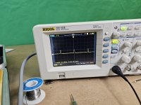
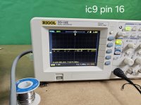
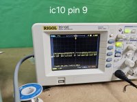
On a RESET you should observe 
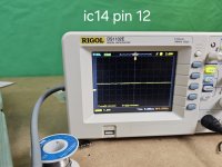
one quick pulse on each of the clock lines for the LED latches (IC19 pins 1, 13 and 4 pulse HIGH) then a constant stream of activity on the keyboard buffer enable (IC31 pins 1 and 15) going LOW.

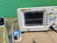
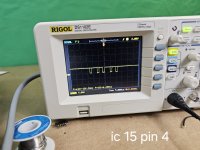
In order to test things out, ONLY depress the 'S' key. This should increment the address by one. By doing one thing (and one thing only to start with) allows us to follow the logic (rather than randomly poking things). Everytime you press the 'S' key, you should observe one pulse on each of the LED latches again, followed by the stream of keyboard buffer activity as the CPU waits for another keypress.

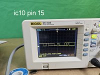
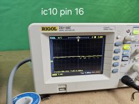
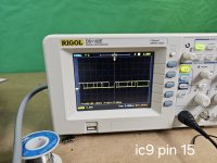
As to your IC18 pin 8. You haven't looked at (and understood) the schematic have you? Address lines A10 through A15 go into SN74LS05 inverters. What is special about these devices? They are OPEN COLLECTOR. You can tell that by looking at the DATA SHEET for the device. Also, notice that all of the outputs are actually connected together! There is a single pull-up resistor (R4) to +5V.

So, when you are measuring pin 8 - this will not just be the inverse of pin 9, but a combination of pins 2, 4, 6, 8, 10 and 12 you are measuring!

So, how does this work?

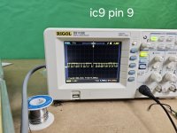
If the address lines A10 through A15 are all logic '0' this means the output from the inverters all all OPEN CIRCUIT. R4 then pulls the signal HIGH. If any of the address lines A10 through A15 is a logic '1', then the inverter output is a logic '0' and it pulls the signal down to logic '0'. The internal active transistor of the inverter gates will ALWAYS win. So ANY logic '1' on address lines A10 through A15 will cause the output signal to be a logic '0'.

So, what you are observing on your oscilloscope is a combination of all of these gates. The signal should only go to a logic '1' when the EPROM or RAM is selected. Which should (actually) be the majority of the time...

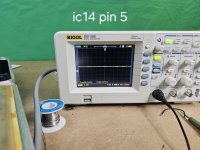
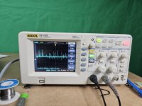
By the way, you have paid full price for the oscilloscope, so you may as well use the whole screen to observe the signal, not just one vertical division. It doesn't cost anymore :)!

Dave
 
Last edited:
So, a bit more thought later...

After a power-up (or a physical RESET) you should observe:

IC15 pin 14 (EPROM) low-going pulses. This indicates that the EPROM is being selected when LOW.

IC9 and IC10 pin 15 (RAM) low-going pulses. This indicates that the RAM is being selected when LOW. This should happen all the time with CPU stack accesses (e.g. PUSH/POP/CALL/RET instructions).

IC9 and IC10 pins 9 and 16 (RAM) should all have pulses on them (memory read and memory write). Again, active LOW.

IC14 pins 5 and 12 should both be HIGH (these are the active low chip selects for the second EPROM and the expansion RAM - neither of which should be selected by the currently executing EPROM).

When you press the physical RESET button (or the 'S' key) you should observe a single HIGH pulse occurring on each of IC19 pins 1, 13 and 4 as data is latched into the LED latches. Use the oscilloscope 'single shot' trigger for this. If the oscilloscope does not trigger - no pulses... If the oscilloscope does trigger - you should observe one pulse.

IC31 pin 15 should be pulsing LOW (virtually continuously) whilst waiting for a keypress.

This would indicate normal (and correct) quiescent behaviour for the board. If any of your tests indicate otherwise, this would be a place to start looking...

I haven't yet found a 'sensible' tiny BASIC (they all require much more RAM than is available). I have found a VTL-2 interpreter (and it assembles OK for the MCS-85). Just looking at the RAM requirements now... (See: https://deramp.com/downloads/mfe_ar...rds/00-MITS/40-Software/minolvtl/mitsvtl2.txt).

Dave
 
Last edited:
Hi Dave,

Got tied up with work. But here are results, each pic labeled.

When you press the physical RESET button (or the 'S' key) you should observe a single HIGH pulse occurring on each of IC19 pins 1, 13 and 4 as data is latched into the LED latches. Use the oscilloscope 'single shot' trigger for this. If the oscilloscope does not trigger - no pulses... If the oscilloscope does trigger - you should observe one pulse.

Haven't quite figured out how to do this yet... is this where I connect up to the actual trigger port? Gotta read up on that.

Also IC31 Pin 15 is stuck HI.

I thought I was gaining an understanding of how it works finally but now I feel like I'm out in the weeds again. I've tested so many connections between pins and they seem good.
 

Attachments

  • 20240110_200806.jpg
    20240110_200806.jpg
    3.3 MB · Views: 5
  • 20240110_200926.jpg
    20240110_200926.jpg
    3.6 MB · Views: 2
  • 20240110_200935.jpg
    20240110_200935.jpg
    3.6 MB · Views: 1
  • 20240110_200948.jpg
    20240110_200948.jpg
    3.5 MB · Views: 2
  • 20240110_200958.jpg
    20240110_200958.jpg
    3.4 MB · Views: 1
  • 20240110_201218.jpg
    20240110_201218.jpg
    3.6 MB · Views: 1
  • 20240110_201243.jpg
    20240110_201243.jpg
    3.4 MB · Views: 5
  • 20240110_200640.jpg
    20240110_200640.jpg
    3.4 MB · Views: 5
Last edited:
>>> Haven't quite figured out how to do this yet... is this where I connect up to the actual trigger port? Gotta read up on that.

No, you don't need to use the trigger port. Use the Y1 input as normal but set the sweep to Single.

See page 2-36 of https://forum.vcfed.org/index.php?t...er-to-other-side.1245325/page-11#post-1360005.

1704965579849.png

In this mode, when the trigger situation occurs, a single waveform will be taken and then stop for you to evaluate the waveform. You will also need to set up the slope setting. If you are looking for a HIGH-going pulse, you need to set the slope to Rising - otherwise you will not see it on the screen!

Also, read page 1-10 on compensating probes.

Dave
 
You have missed IC15 pin 14 out (the EPROM chip select line). And a few of the others also (for example, we have IC10/15 but not IC9/15). Can you just double check that you have done everything I have asked for.

IC31 pin 15 being stuck HIGH indicates that the keypad port is not being read. I am also wondering (as you have not taken the trace yet) whether this extends to the LED latch signals?

Please increase the sensitivity of the Y channel. You are only using a very small part of your screen. If you are measuring a single signal use the whole of the screen...

Once I get some sensible results - we can look in more detail at what is indicated as not working. It does (however) look like the CPU/EPROM/RAM is actually working - but (once I get your results) we can confirm this.

Dave
I mislabelled the last pic. That is IC15 pin 14, not 4.

I see the forum software did not upload my ic9 pin 15 pic. I'll attach it shortly. I'm pretty sure I got everything except what required single shot trigger.

When you say 'use the whole screen', are you saying dial the Y into the shortest possible time base? Like 'zoom' it all the way in?
 

Attachments

  • 20240110_200752.jpg
    20240110_200752.jpg
    3.7 MB · Views: 2
>>> I mislabelled the last pic. That is IC15 pin 14, not 4.

So the EPROM is being selected then.

>>> I see the forum software did not upload my ic9 pin 15 pic.

That's fine also.

>>> When you say 'use the whole screen', are you saying dial the Y into the shortest possible time base? Like 'zoom' it all the way in?

There is nothing to adjust with the timebase, this is the Y (Volts per division) setting of the oscilloscope. The 0V to +5V signal is only occupying one (1) vertical division. I am therefore assuming you either have the X10 set by mistake on your probe or you have the sensitivity set at 5 V/div. Either switch the probe to X1 or adjust the Y sensitivity to 1 V/div. This would mean that the signal would occupy 5 divisions (vertically) on the screen so all of us with poor eyesight can see what is going on better!

Dave
 
I've set the Y probe sweep to single, dialed in Y considerably. I'm still not sure I understand what I'm doing here.. the scope keeps stopping itself, even without me pressing S, but I see nothing onscreen. On one round it didnt do that, but pressing S or RESET produces nothing or no change onscreen.
 

Attachments

  • 20240111_081520.jpg
    20240111_081520.jpg
    3.8 MB · Views: 2
>>> I mislabelled the last pic. That is IC15 pin 14, not 4.

So the EPROM is being selected then.

>>> When you say 'use the whole screen', are you saying dial the Y into the shortest possible time base? Like 'zoom' it all the way in?

There is nothing to adjust with the timebase, this is the Y (Volts per division) setting of the oscilloscope. The 0V to +5V signal is only occupying one (1) vertical division. I am therefore assuming you either have the X10 set by mistake on your probe or you have the sensitivity set at 5 V/div. Either switch the probe to X1 or adjust the Y sensitivity to 1 V/div. This would mean that the signal would occupy 5 divisions (vertically) on the screen so all of us with poor eyesight can see what is going on better!

Dave
Yes in my pic above I brought the voltage down to a much smaller amount per division as pictured above. I don't see any reaction at all to RESET or S on pins 1, 13 or 4 of IC19
 
By RESET, which button are you pressing?

Do you see activity on the CPU pin 12 (RESET) when you press the RESET button or not? The CPU pin should go HIGH when you press the RESET button and LOW when you release it.

Dave
 
By RESET, which button are you pressing?

Do you see activity on the CPU pin 12 (RESET) when you press the RESET button or not? The CPU pin should go HIGH when you press the RESET button and LOW when you release it.

Dave
Yes. RESET has been verified at pin 12 on the CPU, the 8224, etc. I can see all activity ceasing on many other pins while RESET is held and then resuming when released, if that helps.
 
Back
Top