• Please review our updated Terms and Rules here

Plugging in power to other side..

Final note for the day - I was curious why when the machine is powered up it always has the same data (000) on the Port 2 leds, which display what you're typing. I thought initially maybe the 0 key or something was stuck, given the keypad is a little bit dicey. Nope.. but pressing 0 did cause some strange things to happen.. the address leds changed or glitched, and sometimes the machine 'crashed' and would not return to address 3 on reset.

I suspect this is more faulty connections. I've already repaired 10, so this is not surprising.

I also checked connections from the 74174 to IC 2 and 3.. these all checked out.

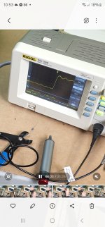
I did hook up a second probe to check IC31 pins 1 and 5. Pin 1 was LOW, I don't know what to make of pin 15. In the pic, pin 1 is in blue, pin 15 is yellow. It held that curve as long as I held the probe to that pin.
 

Attachments

  • Screenshot_20240107_225300_Gallery.jpg
    Screenshot_20240107_225300_Gallery.jpg
    1 MB · Views: 3
A lot of work done yesterday!

Your IC30 pin 9 being 1 Volt is not good. I see the word 'guess' appears in your text!

Check out https://en.wikipedia.org/wiki/Logic_level. This indicates that a logic '0' is guaranteed if the Voltage is < 0.8V and a logic '1' is > 2.0 Volts. It is anyone's guess what it is between these levels!

I see you went on a 'snakes and ladders' expedition with this PCB track! Is the voltage now sensible on IC30 pin 9?

IC 31 pin 1 being permanently LOW is actually a surprise... It shouldn't be! If you look at the schematic for the CPU, you should see that the address lines A0 through A7 go through a set of eight 74L04 inverters and then through a set of eight 7404 inverters, with A0, A1 and A2 going to IC18 pins 15, 14 and 13 respectively. You should chase these signals through with your oscilloscope. They should all be pulsing between (as you now know) a logic 0 level should indicate < 0.8V on your scope and a logic 1 level should indicate > 2.0V. However, I would really expect a logic 1 to be indicating > 4.5V in reality.

I would also check IC31 pin 12. This should be oscillating also. This pin should decode A3-A7 for a port range of 0 through 7 (i.e. A3-A7 as all logic '0').

Your IC 31 pin 15 actually looks OK. When a logic signal changes state, it can 'ring' a bit. This is fairly low frequency ringing, and is normal on old computers! However, it could also be caused by your oscilloscope probe. Did you read up on calibrating your oscilloscope probe before using it? Probably not! Perhaps now is a good time to read up on this procedure and to carry it out... If your oscilloscope probe is not calibrated properly, it can indicate things that are not actually present...

Probably more duff connections to go... You are doing well though based on the number of duff connections you have found and fixed!

Dave
 
Just a point of clarification.

The machine doesn't reset to 3. It resets to address 0. What is displayed on the address LEDs should be 003 000 on start-up. This is the start address of the RAM, and is configured by the contents of the EPROM. This indicates that the EPROM is actually doing something correctly on a reset.

The data that is displayed should be what is in the first byte of the RAM. If you have powered the machine up - this byte will (in all probability) be the same value every time you power the machine up - but this is not guaranteed. If you have already entered some data into the first location of the RAM (using the 'S' key) this data should be retained over a reset (but not over a power cycle).

If you are having problems with the keyboard, it is also likely that you are having problems with the LED displays also. The keyboard is read by the processor inputting a byte from port 0. The three banks of eight LEDs are written to by the processor outputting a byte to either port 0, port 1 or port 2. The same address decoding logic is used for both types of transactions.

Dave
Yes sorry that is what I meant - just that the user always starts at address 003. I think I was borrowing the wording from the article.

Just quickly before work - I checked IC31 Pin 1 and it is oscillating now. I also made a discovery - I noticed the 7442 was a little bit loose in socket, so I pressed it down. Immediately the machine froze up, and on reboot would not go to 003 as the ROM is supposed to make it do. I then gently flexed the board in that area; just above IC 31 in that area where there's a ton of 'through' holes which are linked from one side of the PCB to the other by those little metal 'nails' I mentioned.. and I got it back. While continuing to press on that spot, I tried typing on the keypad and the LEDs on the right started to respond! Not correctly, but lighting as I pressed keys.

Which is good news bad news.. good news is, I think I've found a big part of the problem. The bad news is, there's literally dozens of those little 'nails' connecting one side of the board to the other. It could be a very long repair process to fix all of them. And it might not even be those, it might be bad solder pad connections, bad pins.. this could take a very, very long time to fully resolve.
 
I have just entered the KEX assembly code into the asm80.com assembler. I have coded the comments myself. I have also translated the mnemonics into 'real' 8080 mnemonics. There may be a few typographical errors of course. I have also tried to make the constants a bit more 'assembler friendly' - but I haven't fully achieved this yet...

Code:
ROM     EQU     0Q

RAM     EQU     01100Q

RV10    EQU     RAM + 010Q
RV20    EQU     RAM + 020Q
RV30    EQU     RAM + 030Q
RV40    EQU     RAM + 040Q
RV50    EQU     RAM + 050Q
RV60    EQU     RAM + 060Q

TOS     EQU     02000Q

P0      EQU     0
P1      EQU     1
P2      EQU     2

DELAY   EQU     0446Q

    ; The following jumps vector into RAM to enable
    ; user programs to use the restart instructions
    ; and/or hardware interrupts.
 
    .org    ROM + 000Q
    JMP     START
 
    .org    ROM + 010Q
    JMP     RV10
 
    .org    ROM + 020Q
    JMP     RV20
 
    .org    ROM + 030Q
    JMP     RV30

    .org    ROM + 040Q
    JMP     RV40

    .org    ROM + 050Q
    JMP     RV50

    .org    ROM + 060Q
    JMP     RV60
 
    ; Start of main program.
 
    .org    ROM + 070Q
 
START:
    LXI     SP,TOS      ; Set the stack pointer to the top of
                        ; RAM (actually, one byte higher because
                        ; the stack pointer is automaticcaly
                        ; decremented before use.
 
    LXI     H,RAM       ; The initial value for HL is the start
                        ; of RAM.
                     
POINTA:
    MOV     C,M         ; Load the memory data into a temporary
                        ; data buffer (register C).
                     
    MOV     A,H         ; Output the high byte of the memory
    OUT     P1          ; address to the diagnostic LEDs.
 
    MOV     A,L         ; Output the low byte of the memory
    OUT     P0          ; address to the diagnostic LEDs.

POINTB:
    MOV     A,C         ; Output the temporary data buffer
    OUT     P2          ; to the diagnostic LEDs.
 
POINTC:
    CALL    KBRD        ; Wait and input next key closure.
 
    CPI     010Q        ; Is the value numerical (0..7)?
    JNC     POINTD      ; Jump if a command.
 
    ; The detected keypress was numerical (0-7).
 
    MOV     B,A         ; Save the keycode into reister B.
    MOV     A,C         ; Get the 'old' data value.
    RAL                 ; Rotate 1 bit to the left.
    RAL                 ; Rotate a total of 2 bits to the left.
    RAL                 ; Rotate a total of 3 bits to the left.
    ANI     0370Q       ; Mask out the least significant octal digit (11 111 000).
    ORA     B           ; 'OR' in the new octal digit.
    MOV     C,A         ; Put the new data value back into the buffer.
    JMP     POINTB      ; Take action (output the new data value to the LEDs).
 
POINTD:
    CPI     011Q        ; Is the keypress the "L" command?
    JNZ     POINTE      ; Jump if not.
    MOV     L,C         ; Store buffer data into the low byte of the address (register L).
    JMP     POINTA      ; Take action (output the new address and data value to the LEDs).
 
POINTE:
    CPI     010Q        ; Is the keypress the "H" command?
    JNZ     POINTF      ; Jump if not.
    MOV     H,C         ; Store buffer data into the hgh byte of the address (register H).
    JMP     POINTA      ; Take action (output the new address and data value to the LEDs).
 
POINTF:
    CPI     013Q        ; Is the keypress the "S" command?
    JNZ     POINTG      ; Jump if not.
    MOV     M,C         ; Store the data buffer into memory.
    INX     H           ; Increment the memory pointer.
    JMP     POINTA      ; Take action (output the new address and data value to the LEDs).

POINTG:
    CPI     012Q        ; Is the keypress the "G" command?
    JNZ     POINTC      ; Jump if not. Basically, ignore the command.
    PCHL                ; Go and execute the program specified by the address register HL.
 
    ; We should never get here!
 
    .org    ROM + 0277Q
 
    ; This 10 millisecond delay does not corrupt any registers or the flags.
 
TIMOUT:
    PUSH    PSW         ; Save CPU flags.
    PUSH    D           ; Save the registers that are used within the subroutine.
    LXI     D,DELAY     ; Load DE with the desired delay count for 10 milliseconds.
MORE:
    DCX     D           ; Decrement the DE register pair.
    MOV     A,D         ; Check to see if registers D and E are zero (0).
    ORA     E           ; Ditto.
    JNZ     MORE        ; If DE is none zero, keep looping until it is.
    POP     D           ; Restore DE from the stack.
    POP     PSW         ; Restore the CPU flags from the stack.
    RET                 ; Return from the TIMOUT subroutine back to the caller.
 
    ; The KBRD subroutine debounces key closures and translates key codes.
 
KBRD:

    IN      P0          ; Input from the keyboard.
    ORA     A           ; Set CPU flags appropriately.
    JM      KBRD        ; Loop if key still pressed.
    CALL    TIMOUT      ; Wait for 10 milliseconds.
 
FLAGCK:
    IN      P0          ; Input from the keyboard.
    ORA     A           ; Set CPU flags appropriately.
    JP      FLAGCK      ; Loop if no key press.
    CALL    TIMOUT      ; Wait for 10 milliseconds (debounce).
 
    IN      P0          ; Input from the keyboard.
    ORA     A           ; Set CPU flags appropriately.
    JP      FLAGCK      ; Loop if key not pressed (false alarm).
 
    ANI     017Q        ; Mask out everything except the keycode itself (00 001 111).
    PUSH    H           ; Save HL onto the stack.
    MVI     H,0         ; Zero into the H register.
    ADI     0360Q       ; Add the address of the beginning of the table to the keycode.
    MOV     L,A         ; Store into the L register.
    MOV     A,M         ; Indexed byte from table into A.
    POP     H           ; Recover HL from the stack.
    RET                 ; Return from the KBRD subroutine.
 
TABLE:
    DB      000Q        ; '0'.
    DB      001Q        ; '1'.
    DB      002Q        ; '2'.
    DB      003Q        ; '3'.
    DB      004Q        ; '4'.
    DB      005Q        ; '5'.
    DB      006Q        ; '6'.
    DB      007Q        ; '7'.
    DB      013Q        ; 'S'. Store/See...
    DB      000Q        ; Never generated. No button!
    DB      017Q        ; 'C'. Unused.
    DB      012Q        ; 'G'. Go...
    DB      010Q        ; 'H'. High byte of address...
    DB      011Q        ; 'L'. Low  byte of address...
    DB      015Q        ; 'A'. Unused.
    DB      016Q        ; 'B'. Unused.

    .end

I may do a version for a 3-chip MCS-85...

Dave
 
Since I did whatever I did, now when I press a key you can see some of the correct code coming up on the Port 2 LEDs. Here is a video. We have the same 'bits' stuck every time the machine is powered on or reset, but you can see others changing. There is no evidence though that anything I attempted to enter into memory is actually being deposited there.

I suppose the hint is in the 'code' constantly being displayed on Port 2 - 160. Something somewhere is stuck, the numbers being entered are not shifting left like they should.

I'm not clear on how much problems with the display affect everything else. ie... if it doesn't display properly on port 2, does that prevent the machine from receiving the data at all? Can you have a situation where the data display is not working properly, but the machine is still able to enter data as received?
 
Last edited:
>>> this could take a very, very long time to fully resolve.

But worth it...

Dave
For sure.. I mean, already this thing is doing more than it's done in probably decades, so that's a victory in and of itself. My only concern is that without overhauling all of it, I might be chasing gremlins like these forever, as more links fail.
 
You seem to be randomly pressing buttons... You really need to press the buttons in a logical sequence...

Try pressing the 'S' key. The address should increment every time you press the 'S' key.

The 'C', 'A' and 'B' key do not do anything.

Dave
 
I would also suggest looking at IC19 pin 1, 13 and 4. These are the signals causing the data bus contents to be latched into the LED latches.

It is interesting that the value changes when you press a button, but then rapidly changes back to a default value when you release the button.

Dave
 
Also, is it at all significant that where the address 003 is being displayed, the bit that represents 2 is at 3/4-1/2 intensity as the 1 bit? There is a very fast but noticeable alternation in brightness, like it's changing states very rapidly. The 1 bit is solid and bright.
 
This sort of agrees with what I am thinking in that the LED latches are being selected when they should not be - and this is causing other things to be latched onto the LEDs.

Dave
 
Thanks Dave.

I'll start with ic19 and see if I can figure this out. I'm thinking my strategy of brute force vetting each trace via the schematic is probably my best course of action after that, although that won't help me if we have an accidental short somewhere.
 
I have recast the KEX code (now called KEY) for use on a 3-chip MCS-85 system consisting of an 8085 CPU, 8755 and 8156.

The 8755 has 2K of EPROM (only 256 bytes used at present).

The 8156 has 256 bytes of RAM.

The two devices contain the I/O ports to drive the address and data LEDs (via current limiting resistors) and an input port for the keypad (and associated encoding logic). I will see if I can think of a way to get rid of the external encoding logic for the keypad...

Dave
 
I don't know if this is anything significant.. but after noticing a couple of the legs of IC4 (going by memory.. its a 74174) were not making good contact with the pins there, I corrected. Now the data LEDs are ALL lit.

Unfortunately my poking around seems to have aggravated it. Now it will not 'boot' and go to address 3 without pressure applied near the port 2 7475s. If you let off it 'crashes' to a random address and js totally unresponsive. Press in the right are and it suddenly goes back to address 03.

I have been tracing traces to check continuity.. no problems so far so no idea what is causing this. Maybe next is to test from top IC pins to IC socket pins for each chip.

Also one other thing. The -5v for the 8080 comes in at -4.75v.. is that any sort of problem?
 
>>> Also one other thing. The -5v for the 8080 comes in at -4.75v.. is that any sort of problem?

Both too low and too high voltages are bad news for ALL chips.

Too high because of excessive heat dissipation, reduction in life expectancy and (ultimately) death.

Too low because the part can fail to operate correctly.

You need to go for the 'goldilocks' Voltage - as close to design as practicable.

How do we know what that is? Well, the data sheet for the part describes this. If you look at the data sheet for the 8080 CPU you should observe that VBB (the -5V rail) is specified as -5V +/- 5%. This equates to -4.75V to -5.25V. You are, therefore, right on the edge of acceptable. Too close for comfort to me.

The IN751A is a 5.1V Zener diode - so I am surprised that the voltage is so low.

Also, just measuring the voltage with a multimeter is not good enough... If you have an oscilloscope, this is the best way to measure the voltage. First, with the oscilloscope set to DC. Secondly, with the oscilloscope set to AC and an increased sensitivity on the Y channel. What you are doing now is measuring power supply ripple and noise and not the DC level.

The ripple is a low frequency perturbation that arises at either the mains frequency or twice the mains frequency (depending upon whether the PSU is half-wave or full-wave rectified. This test is for the adequacy of the PSU, the rectifier diodes and the smoothing capacitors (in a linear power supply at least).

The noise arises from logic switching. You increase the timebase frequency and look at the peak to peak noise. Look for the HIGHEST peak to peak noise level.

You can then divide the worst peak to peak voltage by 2 and both add and subtract that from the DC voltage. Look to see if the results exceed the data sheet limits. If so, you could be in trouble...

I assume you haven't tested the decoupling capacitors? The ripple and noise test will see how good they are!

I would next check pins 4 and 13 of the 7475 latches used for the address and data LEDs. I would expect to see short, high-going pulses to latch whatever is on the data bus into the latches. These latches become transparent (will pass through whatever is on the data bus to the LEDs) if the signal is HIGH.

Dave
 
I have revamped KEX for the 3-chip MCS-85 now.

I have tweaked KEX now and found some spare space within the 256 byte EPROM. Since I had some spare space, I have added a new command ('C'). This resets the address pointer back to the start of RAM. I still have some bytes left, so I am thinking of new commands for the 'A' and 'B' buttons... Any thoughts?

I have decided to use the SN74C922 keyboard encoder instead of the separate chips.

What about:

A - Save the memory pointer (HL register) into DE.
B - Restore the memory pointer (HL register) from DE.

This will allow a start address of some memory to be loaded into HL and the address remembered for easy use later.

EDIT1: Added. I still have 18 bytes remaining (in the original 256 bytes). I can remove the key look-up table and increase this to 34 bytes. Just thinking about adding a command for the button that is missing... There is plenty of spare EPROM of course (we have 2048 bytes instead of 256 bytes in the 1702A). I have mapped all of the EPROM into the memory map, so the RAM starts a bit higher than it did in the original.

EDIT2: I have added an additional button (the one that is currently missing) that I have called 'Z'. This command starts execution within the first byte of the spare EPROM (address 001,000). This provides a quick way to execute any additional programs stored in the extra 1.75K of EPROM! Now, do I add an extended debug monitor or some games to the 1.75K of spare EPROM?! Tiny BASIC?!

Dave
 
Last edited:
I am beginning to think that removing the 8080 CPU (thus exposing the address bus, data bus and control bus) and manually driving/monitoring these signals will help isolate the fault to a sub-section of the circuit.

Let me think a bit about this and see if I can come up with something relatively simply...

Dave
 
I have revamped KEX for the 3-chip MCS-85 now.

I have tweaked KEX now and found some spare space within the 256 byte EPROM. Since I had some spare space, I have added a new command ('C'). This resets the address pointer back to the start of RAM. I still have some bytes left, so I am thinking of new commands for the 'A' and 'B' buttons... Any thoughts?

I have decided to use the SN74C922 keyboard encoder instead of the separate chips.

What about:

A - Save the memory pointer (HL register) into DE.
B - Restore the memory pointer (HL register) from DE.

This will allow a start address of some memory to be loaded into HL and the address remembered for easy use later.

EDIT1: Added. I still have 18 bytes remaining (in the original 256 bytes). I can remove the key look-up table and increase this to 34 bytes. Just thinking about adding a command for the button that is missing... There is plenty of spare EPROM of course (we have 2048 bytes instead of 256 bytes in the 1702A). I have mapped all of the EPROM into the memory map, so the RAM starts a bit higher than it did in the original.

EDIT2: I have added an additional button (the one that is currently missing) that I have called 'Z'. This command starts execution within the first byte of the spare EPROM (address 001,000). This provides a quick way to execute any additional programs stored in the extra 1.75K of EPROM! Now, do I add an extended debug monitor or some games to the 1.75K of spare EPROM?! Tiny BASIC?!

Dave
I vote for Tiny BASIC!
 
Back
Top