• Please review our updated Terms and Rules here

RAMdisk under CP/M 2.2

Well, best I can do is an o'scope. I've completely replaced all the memory chips and both '244 buss drivers. I removed all but the first memory chip in the hope it was a loading issue. Interestingly, a previous test I ran left the FF pattern in memory when it was completed. I whipped up a quick BASIC program (slower and 'no assembly required') and sure enough, it read all FF's without issue. So, I think I'm going to run a test where I write a pattern to the memory cells, but instead to reading them to be converted for display, I'll write them to system memory. Then I can just read them from the routine in the system monitor. I'm just trying to get all the info I can.
 
Instead of writing "Patterns" to the memory, try writing text.... At the moment, you're looking for fine detail failures instead of course ones - Just try writing a text document to the memory and reading it back- it will give you a much better idea of the scope of the issue and how much it affects the memory.

A cheap logic analyzer costs $10 and will do 8 channels at around 10 to 20 Msps. It's fast enough for what you want to do and will eliminate any timing issues you might have. If you are building logic circuits and debugging them on this scale, it's a useful tool. If I had to make stuff like this and I didn't have a logic analyzer, I'd make one... I used to make quite a lot of my own development tools back in the 80s. They weren't great, but they did function and did what they needed to.

OK, on reading through you schematic, RD and WR should both go to the RAM chips buffered and without being gated by the 138, but I can see why you did that as the CS is permanently selected, so you might have a propagation related delay there affecting the RAM timing. Is your oscilloscope dual-trace?

How many nanoseconds before the rising of the clock signal does the WR line to the RAM ( post-propagation delay ) go high before the clock signal rises? You might be delaying the write signal too long with all of the additional combinational logic, especially if there's any significant capacitance on the write output to the RAM?

Anyway, after analysing your schematic, here's why I think it's not working.

You destroy the data signal pretty much immediately via the 244 at the top of the diagram as soon as write goes high, but the write line to the RAM is still low due to the propagation delay through two gates, and the added capacitance of the bus fan-our, so that's a really likely source of error since you aren't keeping the data stable on the lines as the RAM requires ( The 244 will disable the data lines to the Memory BEFORE the write cycle is completed, according to the estimated propagation delay through the system based on your design... ). Hence you are removing the data from the RAM data bus AND THEN you are raising the WR signal high, which should create random data in some cases on the bus, likely related to the strongest capacitive link any of the data bus lines have to any other switching line.

You need to ensure that the data is stable until AFTER the write signal goes high... Hence at the very least as an experiment, run the WR line from the CPU to the Enable lines on the LS244 for the WRITE circuit rather than taking it from the CPU, so at least they occur at the same time, which is still pretty poor, but is likely to work at least.

Regards
David
 
Nope, just realized you have an issue with the registers if you do that since their timing is on the same chain.

Option 1- Have two 74LS244 where U14 is, or run your inputs to the latches input direct since they should have very low load on the data lines and there's only 3 of them, and use the 244 to drive the RAMs.

Option 2 - FInd a way to extend the write signal... That means at the least something like a RC circuit to delay the onset and release of WR - eg, WR through a resistor, then a small CAP on pin 1 and 19 of the LS244.

Option 3 - My favourite,
* Take the RAMSEL line from Pin 11 of U12 ( 74LS138) and run this as the ONLY enable into the 74LS138 at U10 - though you can use the other two as "range" selectors if you like.... But use it to replace G2A or G2B at least.
* Remove the output from Pin11 of U12 away from U16 entirely. Make U16 a FAST PROPAGATION buffer ONLY - ie, don't mess with the outputs via another signal. Use these RD and WR as the only feed to other RD and WR lines in the circuit so that ALL ram chips see RD and WR change at the same time the 74LS244's see it change, or close enough at least.
* Run Pin 11 of U12 to Pin 19 of the two 74LS244 chips - U17 and U14. This way the buffers only work while both signals are present. Same as your present design, but simplifies the timing. ( Leave Pin1 as RD and WR on the chips respectively) and will do the same as your mixing through the OR gates - Also, avoid two inverters as buffers for RD and WR where you can, but if you can't, that's fine... Just make both inputs to each gate (eg, U16 inputs from RD and WR) both go to the same RD or WR signal.

This should address the race condition you're introducing into your circuit design, by having two sets of write timing -
Regards
David

p.s. Nope, that still won't work.. Because of the registers. You need to separate the "Enable" line from the 74LS138 entirely from U14.... Hmmm. OK, Maybe just run the BUFFERED write line to both gate inputs of U14 with Option 3, but leave one gate of U17 to Pin 11 of U12 and one gate of U17 to Buffered READ ...

I think that may be enough to fix the race condition.
 
Last edited:
Well, I'm slowly trying to wrap my head around it. For the first 'bullet' I see running U12-P11 to U10-P5 or P4. The hard part is that the '244 has two sections of four buffers, each with it's own enable. So, Pin 1 & 19 have to operate together. What if I just U14-P1&19 controlled by an inverted /READ signal? That could be worth an easy try....
 
You could just use an inverted RD signal, which would stabilise the bus to the RAM, but may cause a slight race condition between the two buffers and the RAM, though we're only talking residual nanoseconds...

Might be worthwhile as a brief experiment to validate the fix, and would be easy to do ...

Yeah, give it a shot I reckon.
 
I will try it today sometime and see what happens. No harm in trying.. And thanks for the suggestion......
 

Attachments

  • MemoryDiskv6.pdf
    89 KB · Views: 3
I'm curious to the outcome now - Will be waiting with baited breath.

I can be absolutely certain the race condition exists and would explain the issue - but I can't predict if it's enough to cause the issue or if it's the only issue.

David
 
Use the pre-inverted (B) signal to drive the gates for the write buffer, but leave the existing write signal to the latch OR gates that follow the 74LS138 at U12.
 
But if I use the 'pre-inverted (B)', U16-P4, to drive the enables of U14, then it would only provide data to the three latches when I'm intending to write or read data in/out of the memory chips.....

As a side note: when I implement this on my S-100 system, I am going to completely separate the internal data buss that is used for the three address latches from the internal data buss used for actually writing & reading data to & from the memory chips. I think that will be cleaner.
 
It doesn't matter - The inverted RD line will be LOW ALL of the time except when reading from the 74LS244.

That just means the data bus will ALWAYS be reflected on the circuit data bus, whether the chips are being read or not. That shouldn't affect anything I can see in your circuit - Simply put, U14 will be active at all times except when U17 is active.

Since all of your other activites are WRITE activities, that's fine - it shouldn't make a difference. The data for the latches will pass through U14 regardess as RAM-READ is not selected, and the data for RAM-WRITE will also pass through for the same reason.

Regards
David
 
Now my curiousity is raised even further, can you take a picture of your system that you stick all of this into as well? I'd love to see what the whole thing looks like.

:)

David
 
Well, that's a no go on the circuit changes. No change at all. I'm still not 100% convinced it isn't a problem in the code used to display the output. And here's why... When I run the test that leaves FF's in all of the memory locations, and get all the errors; I can run a BASIC program that reads that same FF data and it does not show any errors. Now, BASIC runs slower, but the code it uses to read from a port has to use the same IN a,(xx) as I have in my machine language program. This weekend, I'll change the test program to store the data I read back into system memory. The use the monitor program to dump that data to the screen. If no errors, then I know the issue is in my machine language test program and how reads and displays the data.
 
Perhaps write a subroutine to write a byte, eg, Address in DE and C, and byte in A, then one routine for write and one for read. Once you standardize on a working subroutine for read and write, you only need to call it and you can change the data to whatever you want... And you only need to debug a single routine and a single byte at a time...

something like;

LD B,FF TOP: LD C,0 LD DE,0 LD A,B CALL WRITEBYTE CALL READBYTE CP (B) JR NZ,ERROR DJNZ TOP .... another cycle? WRITEBYTE: PUSH AF LD A,E OUT (45),A LD A,D OUT (46),A LD A,C OUT (47),A POP AF OUT (44),A ret READBYTE: LD A,E OUT (45),A LD A,D OUT (46),A LD A,C OUT (47),A IN A,(44) ret
?
David

p.s. I assumed the ports from the schematic.
 
If the code test doesn't show good results, I think a re-wire to provide separate data paths will be my next experiment. I attached the schematic of what that would look like.
 

Attachments

  • MemoryDiskv7.pdf
    89.3 KB · Views: 5
Perhaps write a subroutine to write a byte, eg, Address in DE and C, and byte in A, then one routine for write and one for read. Once you standardize on a working subroutine for read and write, you only need to call it and you can change the data to whatever you want... And you only need to debug a single routine and a single byte at a time...

something like;

LD B,FF TOP: LD C,0 LD DE,0 LD A,B CALL WRITEBYTE CALL READBYTE CP (B) JR NZ,ERROR DJNZ TOP .... another cycle? WRITEBYTE: PUSH AF LD A,E OUT (45),A LD A,D OUT (46),A LD A,C OUT (47),A POP AF OUT (44),A ret READBYTE: LD A,E OUT (45),A LD A,D OUT (46),A LD A,C OUT (47),A IN A,(44) ret
?
David

p.s. I assumed the ports from the schematic.
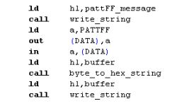
David, kinda what I do. I first setup the three latches (track, sector, & byte), then cycle through the twelve patterns, and display the results as I go...
1682005275233.png
Display what the expected should be, write the data to the already selected address, read it back in, and then display what the actual data read back is. Cycle through all twelve patterns, then move to the next byte; rinse, repeat.
 
If the code test doesn't show good results, I think a re-wire to provide separate data paths will be my next experiment. I attached the schematic of what that would look like.

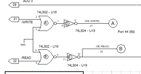
Don't forget to remove the output from the 138 from the buffering of RD and WR - That will get your RD and WR closer to the timing of the z80 and make it easier to debug.

David
 
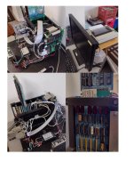
You had asked about my development system....... The CPU board is an SBC from CPUville and I use an old Cisco flash card for storage, Then I have a STD buss card to interface the CPU to the STD buss. There is a front panel board for buss termination, clocks, address, data, and status display. There is a printer card to drive my Panasonic dot matrix printer, and a dual port serial card using 8251A's. I have 5V/10A & +/-15V power supplies to power the thing. The keyboard and display are connected as a terminal to the serial console port via a LegacyPixels device to emulate a VT-100. This is my design and test bed before I build up my S-100 system. Eventually, this will become the smart terminal for my S-100 system.
 

Attachments

  • SystemPictures.jpg
    SystemPictures.jpg
    83.7 KB · Views: 5
Don't forget to remove the output from the 138 from the buffering of RD and WR - That will get your RD and WR closer to the timing of the z80 and make it easier to debug.

David
Oh, for the v7 version... Gotcha. Thanks. As in this instead....

1682007680042.png
 
Back
Top