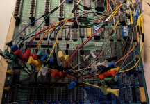
So this board could potentially boot with these roms if I populated all the banks... I have a ton of DRAM here that came with the boards, maybe I'll try to breadboard one of those Arduino RAM testers.
Upcoming Events:
- VCF South West - June 14 - 16, Davidson-Gundy Alumni Center at University of Texas at Dallas
- VCF West - Aug 2 - 3, Computer History Museum, Mountain View, CA
- VCF Midwest - Sept 7 - 8 2024, Schaumburg, IL
- VCF SoCal - Mid February 2025, Location TBD, Southern CA
- VCF East - April 2025, Infoage Museum, Wall NJ
-
Please review our updated Terms and Rules here
- Forums
- Companies
- IBM Computers, PCs, Clones and Descendants
- PCs and Clones (XT and early AT class machines)
You are using an out of date browser. It may not display this or other websites correctly.
You should upgrade or use an alternative browser.
You should upgrade or use an alternative browser.
Fixing Five Festive 5150 Boards over the Holidays (BOARD #3 Thread)
- Thread starter VeryVon
- Start date
modem7
10k Member
You will be talking about a boot into Cassette BASIC.So this board could potentially boot with these roms if I populated all the banks...
And your "all the banks" must be in reference to the issue described at [here], which applies to the the 10/27/82 revision of IBM BIOS ROM. Even with that issue taking effect doesn't mean that you, under no circumstances, can boot to Cassette BASIC. For example, with my 64KB-256KB type motherboard fitted with 10/27/82 BIOS ROM, if I have only bank 0 populated, and set switch banks SW1 and SW2 accordingly, then at startup, I see a '1055 20' error (because of the issue), followed by a boot into Cassette BASIC. Cassette BASIC (version C1.1) shows "12252 bytes free", not the expected figure (of slightly less than 64 KB).
Thanks acgs for commenting here on my behalf! I didn't see your post or I would have thanked you sooner!
As acgs said, I am working on a 5150 based project to redesign one, and a reference board would possibly be helpful to me!
If the owner likes to sell one, maybe I would be interested. Even if a PCB is broken, as long as the PCB is physically looking in good state I would love to have one of these boards.
I am always searching ebay and the like but those prices are really crazy so far.
I saw one PCB for a reasonable price but it was obvious in the photos that it was etched by battery acid or other harmful stuff.
I hope I can be lucky in the future to find a good affordable one.
Anyway, VeryVon your work looks very interesting and cool with the logic analysis. I hope you can fix them all, looks like great fun!
I also own something like that to connect to USB and probe 40 signals but last time I used it on something I was reverse engineering I got some weird inconsistent readings that couldn't be right so I am not sure if it is working properly anymore. I should have another try to test it again, maybe on my project just to see if it can monitor timing events.
Kind regards,
Rodney
Thanks acgs for commenting here on my behalf! I didn't see your post or I would have thanked you sooner!
As acgs said, I am working on a 5150 based project to redesign one, and a reference board would possibly be helpful to me!
Anytime, Rodney. I think all of your hardware updating work, and that of others like @MicroCoreLabs, is important to keeping the use of this era of machines alive. While the original equipment will likely become impossible to save eventually, being able to recreate these computers using modern components means that the using of them never has to disappear. While not the latest and greatest tech out there anymore, their usefulness as computers is still there and the amount of software available is still growing.
Anyway, since you didn't find my comments until now, I guess you can think of them as my little gift to you for this special time of year.
Happy Holidays!
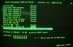
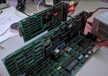
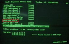
Ok, finally running Ruud's 4.3 With all RAM banks populated! I consistently get failure at Address: 15KB (exactly 03FFC [hex]) I also have the Mini Post Code card connected, it's really cool to see the checkpoints read out on the card 


Hi acgs,
Thanks for your support! I appreciate it, and happy holidays to you too!
VeryVon that is indeed very cool, I definately should try this out too. This kind of readout would even be cool to have as a default feature on a system, I will look into this if it could be an option. Using bank switching I could try to include a switchable diagnostics ROM page in the BIOS EPROM as well. If an XT BIOS supports some output that would even be cooler to show some codes happening from the POST process. I will remember this for later in my projects.
My designs will not need so much diagnostic work or repairs I expect, but it is also simply cool to play around with. I have had ideas before as well to show a detailed display of various signals of the system on a front panel LED connector. Or perhaps probe the bus with a controller like a RP2040 and output on a small display what is going on in the system.
Do I see it correctly now in your screen photo that all 8 bits are in error at that location? If so that would be weird to happen since every bit has it's own separate DRAM chip, is it really caused by the RAM? Or perhaps an address bit having some trouble causing a memory fault? A marginal multiplexer? Or maybe I am not reading the screen or function of diagnostic wrongly? I never used any diagnostics before.
Kind regards,
Rodney
Thanks for your support!
VeryVon that is indeed very cool, I definately should try this out too. This kind of readout would even be cool to have as a default feature on a system, I will look into this if it could be an option. Using bank switching I could try to include a switchable diagnostics ROM page in the BIOS EPROM as well. If an XT BIOS supports some output that would even be cooler to show some codes happening from the POST process. I will remember this for later in my projects.
My designs will not need so much diagnostic work or repairs I expect, but it is also simply cool to play around with. I have had ideas before as well to show a detailed display of various signals of the system on a front panel LED connector. Or perhaps probe the bus with a controller like a RP2040 and output on a small display what is going on in the system.
Do I see it correctly now in your screen photo that all 8 bits are in error at that location? If so that would be weird to happen since every bit has it's own separate DRAM chip, is it really caused by the RAM? Or perhaps an address bit having some trouble causing a memory fault? A marginal multiplexer? Or maybe I am not reading the screen or function of diagnostic wrongly? I never used any diagnostics before.
Kind regards,
Rodney
modem7
10k Member
To make sure everyone is on the same page, this is an address error, not a data error. An address related problem is broadly explained at [here]. The cause may or may not be a RAM chip.Ok, finally running Ruud's 4.3 With all RAM banks populated! I consistently get failure at Address: 15KB (exactly 03FFC [hex])
In testing the 'Testing RAM - Address' test of Rudd's Diagnostic ROM (RDR), I did lots of experimentation, usually lifting up one of the address pins on a RAM chip then tying that lifted pin to ground, or to +5V. Also, things like manipulating bits on the memory address bus. In seeing how RDR reacted in those experiments, I usually saw strange failure addresses (which would have been explained had I done an analysis), and so the address of 03FFC that you see should not be taken to mean the problem cause must be related to bank 0.
Similarly, one must not make assumptions based on the bit/s shown in error. For example, a RAM chip can fail in a way that causes one address bit on the memory address bus to be stuck LOW or HIGH. That will impact on all motherboard RAM chips. On the other end of the spectrum, there have been failure modes where the bit error pattern shown, did point to a particular address-bad RAM chip.
Note that chip testing hardware may or may not do an address test of the RAM chip under test.
A problem on the address bus can impact on the memory address bus. One cannot assume that the address bus is good based on the fact that RDR is executing. To execute, RDR only requires a certain portion of the address bus to be functional.
So I think that the order of diagnosis should be:
1. Prove the address bus (all 20 bits).
2. If that is okay, investigate the memory address bus.
A partial test of the address bus is to use the TEST5065 code at [here]. I used 'partial' because the code will not reveal shorted bits. To detect shorted bits, the code would need to be changed to use addresses AAAAA and 55555, together with the use of a logic analyser. (A multimeter may also reveal low resistance between bits.)
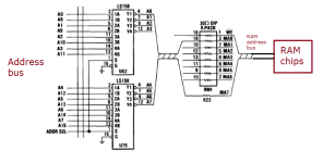
As for the memory address bus, when the 'Testing RAM - Address' test fails, the RAM refresh mechanism is still operating in the background, and so, using a logic probe, expect to see activity on all bits of the RAM address bus. A logic probe though, will not reveal shorted bits.
Come to think of it, per [here], the RAM refresh mechanism is counting up on the address bus using bits A0 through A15, and with a logic probe, you expect to see activity on A0 through A15. (However, again, a logic probe will not reveal shorted bits.)
Interesting what you have done in experimentation modem7. If I have the time, I may do this too just for fun. Having seen more examples of what the diagnostics show can increase diagnostic experience and help to recognize what is wrong when you see a certain type of test result, interesting.
Indeed troubleshooting DRAM is really difficult as they have many failure modes, finding a problem in a system is always difficult because of the interconnections present so the schematic must be rechecked again and again against the test results to estimate what could be going on. It's good to consider stuck bits as a possible cause because it can happen. Using an oscilloscope could be helpful and can also give hints to which signals are failing specifically and for examble might be stuck which you can see in the signal patterns compared to eachother. Like no activity, or seeing weird half levels in one signal in certain points, and not in others. Then it must be considered which chip on the particular signal is doing that. Having a defective IC inside a system is always a complex problem.
Doing a chip test on a DRAM I have also seen examples of test devices showing a good chip which then in the system still is misbehaving. It's good to keep this in mind at all times, indeed. One should never assume any DRAM is good and then think you can move on past that, it's always still a possibility that something is wrong with it and went undetected.
From all this complicated reasoning necessary and complex failures which can possibly happen, I wonder if it would not be better to replace the DRAMS with known good ones and test working backwards with placing the original ICs back. Like putting some stickers on the chips and making a test log which chip is working properly. Arguably this method is perhaps less of a challenge but can save a lot of time.
After finding the offending IC, it could still be interesting to put it back in and try to probe to determine if you can observe how it is disrupting the system. But this is all a matter of preference and goal of the person doing the actual repair in the end. It will be interesting to see your progress and what you discover VeryVon, good luck!
Thanks rodney, could use some! These 5150 bus protocols are nothing to sneeze at, thank god for modem7's diagrams and test code.It will be interesting to see your progress and what you discover VeryVon, good luck!
Thank you for the explanation on "address testing" it riddled my mind for a good day or two, and I didn't realize you have a page dedicated to that. Very well documented.
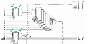
Ok about those address busses, I haven't found any stuck address bits while using the TEST5065 code. I looked at A0-A19 on an ISA slot (great tip btw, all lined up on the right-hand side of the bus there) and I looked at "X" (buffered) address signals on either side of U15, U16 and they're good. I also checked U62, U79 and RN4 (U78) and all good input & outputs.
I went over the ram banks too. Not sure exactly what I should see there running TEST5065, but here are my observations:
- RAS/CAS only active on Bank0
- Address Lines: all active
- Data Lines: I'm getting a mixture of signals here that the logic probe often interprets as a "buzz" neither high nor low. Except for D3 which appears to be steady high. They don't look right on the scope either
- I checked the resistance between all the data lines, they look OK. If it registers on auto range it's something like 32 M Ohms

Last edited:
modem7
10k Member
For those that have a screen display, note that the checkpoints also appear in the top right corner of the screen. Sometimes, that provides possibly relevant information. For example, the B7 shown in your screen shot within post #46, informs me that of the address test, it was the first part (of two parts) that failed.I also have the Mini Post Code card connected, it's really cool to see the checkpoints read out on the card
The ZIP download file of Rudd's Diagnostic ROM (RDR) includes the source code, and so if you really wanted to, you have the ability to predict the failure address before running RDR.Interesting what you have done in experimentation modem7. If I have the time, I may do this too just for fun. Having seen more examples of what the diagnostics show can increase diagnostic experience and help to recognize what is wrong when you see a certain type of test result, interesting.
I think it is rare (comparatively speaking). My last find was two years ago. I recorded it in the bottom table at [here]: "Discovered about 4 ohms between bits 2 and 1 of the external data bus. Tracked down to chip U10, a 74LS670, used for the DMA page registers."It's good to consider stuck bits as a possible cause because it can happen.
That 'Checkpoints' page that you point to includes:Thank you for the explanation on "address testing" it riddled my mind for a good day or two, and I didn't realize you have a page dedicated to that. Very well documented.

Additional information is there, including a link to the 'Memory addressing problem' page.
modem7
10k Member
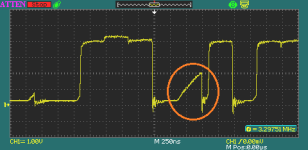
Just be careful about interpreting things using an oscilloscope.Data Lines: I'm getting a mixture of signals here that the logic probe often interprets as a "buzz" neither high nor low. Except for D3 which appears to be steady high. They don't look right on the scope either
For example, the following is an oscilloscope capture of one of the RAM data pins on my good motherboard.
modem7
10k Member
In the ZIP download file is file TEST5065.TXT, and that has a 'WHAT YOU SHOULD OBSERVE' section.I went over the ram banks too. Not sure exactly what I should see there running TEST5065, but here are my observations: ...
So, activity on all 20 lines of the address bus. Good.... Address Lines: all active
The possibility of shorted 'address bus' bits has not been ruled out yet, so that possibility gets put aside for now. Note that 'shorted' adjacent bits cannot always be detected using a multimeter - the short may be very much inside the chip and not presenting to the chip's pins. To test for shorted 'address bus' bits later, 55555 and AAAAA get put onto the address bus, and you verify those addresses via a logic analyser. Setting up a logic analyser is a 'pain'. I tend to knock over what diagnosis I can do using a logic probe, and if that is unsuccessful, then 'bring out the big guns' (the logic analyser).
No, you cannot say that they have good outputs. All you can say is that you observed activity on the output pins. Maybe the activity is 'bad'.I also checked U62, U79 and RN4 (U78) and all good input & outputs.
For example:
1. A test for shorted bits yet to be done. Logic analyser required.
2. U62 and U79 form a multiplexer, creating for the RAM chips, a row address followed by a column address. The timing for that is controlled by the ADDR SEL signal (which you gained confidence in at post #32). Either U62 or U79 could faulty in a way that results in it stuck at using a the 'A' input pins, or stuck at using a the 'B' input pins. Logic analyser required.
modem7
10k Member
Where to now?
Before bringing out the logic analyser, here are my thoughts:
1. You could take a punt and replace U62 and U79 with known-good chips. Even before that, try piggybacking known-good chips on U62 and U79, because sometimes, that can reveal a faulty chip.
2. Bad RAM chips, faulty in a particular way? If I look at post #46, you have all four RAM banks (all socketed) populated. Were you not getting the address error with only one bank populated? If no error, you could continue with 'bank 0 only' operation, and in stages, swap in the other RAM chips into bank 0, expecting that at some point, the address error will appear (probably showing a different address).
Last edited:
Indeed a good point, when I was writing about using the oscilloscope, I also remembered seeing some half voltage signals in my XT design. I forgot to comment about it so thanks modem7 for pointing to this possibility which I also have seen before while debugging my XT.Just be careful about interpreting things using an oscilloscope.
For example, the following is an oscilloscope capture of one of the RAM data pins on my good motherboard.
The half signals can also appear during tristate periods where the signal is not being actively driven by any chip on the mainboard. So the signals are floating or slowly progressing to a certain voltage until they are driven again.
I think a good measure, though not definitive, would be to probe other adjacent signals in the same bus to see if the half signals or other unusual patterns also appear in these. If one bit is showing very different patterns from others it may be indicative of a problem, though the schematic has to be consulted carefully to see if that one bit is not an exception anywhere in the circuit which might also explain the difference. Comparing signals can sometimes point to a problematic one, but it should be approached with careful thinking about how the signal is being driven as it may not point to any problem. Ideally, if you have a known good working "reference" 5150 next to the faulty one, of the same configuration, with the same ROM and RAM population, you could compare possible problematic signals to try to locate where the problem may exist. This could also eliminate signals which appear wrong but may possibly be okay.
I think it is rare (comparatively speaking). My last find was two years ago. I recorded it in the bottom table at [here]: "Discovered about 4 ohms between bits 2 and 1 of the external data bus. Tracked down to chip U10, a 74LS670, used for the DMA page registers."
Very interesting modem7 about the 74LS670 which failed with such a low resistance short. Possibly the chip would also be heating up then, which reminds me that touching ICs may also indicate a problem if they are much hotter than others, like unusually hot. Especially when you sense a certain chip even radiating a lot of heat. Though as you said it is still rare this type of failure. Do you happen to remember who was the manufacturer of that 74LS670? I also always wonder how the condition of failing mainboards is, did they get a lot of exposure to moisture or not for example, which unfortunately can happen due to careless handling and storage. Some of the used boards I bought did suffer from moisture which could lead to failing chips. I don't usually repair many boards because I mostly only build my own stuff and didn't see many old mainboards yet, but I did see a RTC chip fail on my IBM 5170 mainboard, it literally happened during testing, one moment it worked fine, the next moment at power on the RTC had died. That mainboard did show some oxidation on component pins due to moisture influence, including that faulty RTC.
modem7
10k Member
In diagnosis, I established that there was a problem on the external data bus, and eventually deduced that the same signal was always on data bits 1 and 2. That's when I checked using a multimeter and to my surprise, discovered the 4 ohms. I knew that the cause was either a chip or the PCB. In turn, I cut the data bit 1 (or maybe it was bit 2) pin on the chips on the external data bus, and the 4 ohms disappeared when I got to the 74LS670.Very interesting modem7 about the 74LS670 which failed with such a low resistance short.
No.Do you happen to remember who was the manufacturer of that 74LS670?
I used to have many 51xx motherboards, now down to about 8. These are boards that I have had for many years, and are stored well. I make sure they get periodic 'exercise'. Sometimes I bring out a motherboard (that was put away in working state), and discover that it no longer works. Of course, I do not know if the faulty component failed at application of power, or failed during storage.I also always wonder how ...
There have been cases where people with a faulty 5150 motherboard (RAM chips in bank 0 are soldered in) discovered multiple faulty RAM chips in bank 0. I have experienced this myself (on a 5150 motherboard that I acquired). At the point in time when the first bad RAM chip in bank 0 went faulty, the board was unusable and would have been shelved. So, does that mean that the other RAM chips failed whilst the motherboard was shelved? Or was it the case that the motherboard suffered from a power surge, taking out multiple RAM chips in bank 0, and taking out nothing else?
Member bobba84 found 10 faulty RAM chips on a 5160 motherboard that had been stored in a shed for 7 years.
At [here] is shown a faulty diode that I discovered in a moisture affected 51xx PSU. It appears that moisture made its way past the hermetic seal into the diode. Hermetic seal compromised due to age?
An obvious example is shown at [here].
I guess that's where these five boards came from? I'll have to inquire with the original collector to see if he knows more.the board was unusable and would have been shelved
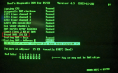
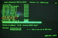
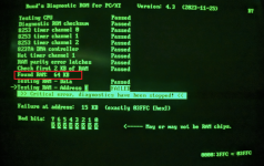
I started removing banks and booting RDR. The same error appears each time. I don't have any known good LS158's here (thought I did, but they're 157's) too bad because I'm always up for a short-cut
I'm getting the gut feeling it's something with the data bus, but I guess that's a pretty broad statement haha. Should we test for "stuck bits" on the data bus?
modem7
10k Member
Which includes 'bank 0 populated only'. Maybe one (or more) of the chips presently fitted to bank 0 is causing the problem. A leg bent up under the chip is a possibility.I started removing banks and booting RDR. The same error appears each time.
( I can see you swapping 'sets' of RAM about at post #36, but that was when you were using a version of RDR that did not check for RAM addressing problems. )
Yes.I'm getting the gut feeling it's something with the data bus, but I guess that's a pretty broad statement haha. Should we test for "stuck bits" on the data bus?
If you are capable, you can modify the TEST5065 code to output addresses AAAAA and 55555. An oscilloscope will be good enough to detect shorted adjacent bits.
But I certainly plan to do that modification (very shortly), creating TEST5066. Included in the ZIP file for TEST5066 will be logic analyser captures of the address bus, and the memory data bus.
Legs look fine, and I checked the underside of the board under the scope again, can't find any obvious problems. However looking at the chips in the sockets under the scope, some of the leg's aren't touching the outside socket wipes. They're double-wipe but it's not giving me super confidence, I wonder if these are the cheaper type of sockets one gets on amazon. I can see why people switch exclusively to machine pin sockets, and I've considered it myself. I'll do some more recon to verify conductivity, I've seen more than one war story out there about flakey sockets causing people to pull their hair out.A leg bent up under the chip is a possibility
I'd certainly like to be. I downloaded nasm-2.16.01, and ran this to attempt to duplicate your binary:If you are capable, you can modify the TEST5065 code to output addresses AAAAA and 55555
nasm -f bin TEST5065.asm -o TEST5065.BINIt produced a file very similar to yours, with a few differences. Unsure if functionality is equivalent, guess I'll have to burn it to an eprom and see if the address bus is toggling heheh.

Last edited:

