• Please review our updated Terms and Rules here

Starting my first Pet, a 4032 in desperate need of some love

It might be worth repeating the UE12 output testing again then - monitoring each pin for a good few seconds.

The tests are (in order):

Video RAM (so you shouldn't see activity on the /0 output during this time). I wonder if you will though? It depends upon your oscilloscope and measuring technique - and you seem to be good at this - so you may observe some activity on the /0 output...

Page 0 and 1 RAM - it could be stuck here (good old 4116 DRAM errors).

ROM checksums - you should be able to see some activity on the ROM /CS pins (outputs from UE12 anyhow). This will timeout after 60 seconds or so and enter the full DRAM tests (if you get this far).

Full DRAM test - you should see plenty of activity on UE12 outputs /0 through /7.

Dave
 
I do have a B128-80 but it looks like a different chip (80 col?) and its soldered anyways.

I thought I would get better at Pets before tackling this thing. It has no screws in it and is likely not working.

Mike
 
It might be worth repeating the UE12 output testing again then - monitoring each pin for a good few seconds.

The tests are (in order):

Video RAM (so you shouldn't see activity on the /0 output during this time). I wonder if you will though? It depends upon your oscilloscope and measuring technique - and you seem to be good at this - so you may observe some activity on the /0 output...

Page 0 and 1 RAM - it could be stuck here (good old 4116 DRAM errors).

ROM checksums - you should be able to see some activity on the ROM /CS pins (outputs from UE12 anyhow). This will timeout after 60 seconds or so and enter the full DRAM tests (if you get this far).

Full DRAM test - you should see plenty of activity on UE12 outputs /0 through /7.

Dave
I am clearly not understanding something here. On the 74154 outputs 0-3 on pins 1-4 have no connection on the schematic and, I see none on either side of the board. /0 output does have activity but is not connected anywhere?

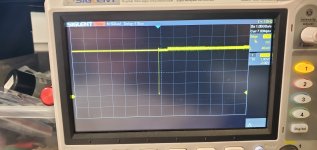
I do see a brief signal on Pin 17 (/SEL-F) which selects the first ROM on the schematic - UD6. I can't see it unless I set a trigger and it takes a couple seconds to show up. I have yet to figure out how to check for subsequent triggers to see if this repeats. It does only happen after a reset but never on the machine after it has been running for a few seconds. Interestingly the 5V on /SEL-F is very clean until the /CS signal and is pretty dirty afterwards. I am not certain if that is just because the line has not yet stabilized or is the chip being selected causing issues.

20230321_135720 - SEL-F on 74154.jpg
1V 500uS / div (Zoomed out to see ugly, but still OK TTL, afterwards)

That reminds me, where do I look to see which ROM is which? The BoM only lists them as 2316s adn the schematic only shows what address they map to (This one is F000-FFFF)

Mike
 
If I have understood your question correctly:

In a PET with a four-ROM set, usually:-
UD6 - BASIC ROM (1 of 2) base address, C000h
UD7 - BASIC ROM (2 of 2) base address, D000h
UD8 'Edit' ROM, base address E000h *
UD9 'Kernal' ROM, base address F000h (most people, especially Linux people, would spell that 'Kernel').

* The 'Edit' ROM UD8 only has half the capacity of the other ROMs UD6, UD7, UD9 and resides in the lower half of the E000 block. The peripheral ICs are mapped into the upper half of the E000 block at E800 onwards. See also the notes in the next post by Daver2.

Each of the ROMs should have a long number printed on the top which is specific to that ROM and its contents. Usually the long number will have the form 90xxxx-xx

Once you've read that number off each of your ROMs you can look them up by scrolling down this page here:-


Bear in mind that all of the above information is based on my fairly limited experience with PETs, your machine may not conform but as far as I know this ROM memory map has been adhered to quite consistently across the PET range. If you have a PET with a 5-ROM set (With BASIC 4?) then usually the extra ROM will be UD5, base address at B000h, and that is another BASIC ROM. Occasionally a previous owner will have added a fifth ROM to what was originally a 4-ROM set and if they have that will usually be a utility ROM of some sort, and it may be placed in the UD5 position.
 
Last edited:
The UD8 (EDIT) ROM lives at $E000 to $E7FF. The I/O area starts at $E800. Later PETs then carry on the EDIT ROM from $E900 upwards (i.e. the EDIT ROM can be a 4K ROM with a 'hole' for the I/O devices).

When the 6502 is reset, the program counter is loaded from the 8-byte area right at the TOP of memory. In the Kernal ROM, this starts executing a bit of code in the Kernal ROM before transferring control to the EDIT ROM.

If you have my PETTESTER installed, this is how I take over control of the machine!

The initial /SELF pulses you observe immediately following a reset condition is the CPU reading the reset vector (to load into the Program Counter) and for the initial few instructions before the Kernal ROM calls the EDIT (PETTESTER) ROM where I hijack the CPU.

Dave
 
I guess I was thinking more in terms of schematic than IC. I have looked some up on zimmers in the past. I will print Sirius' notes and add them to my service manual

Mike
 
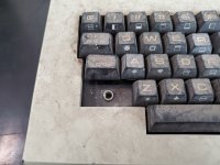
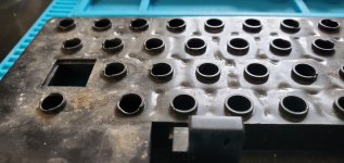
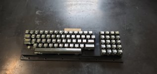
While waiting for the CRTC I thought I would get some of the cosmetics taken care of. I also thought I would get the Keyboard restored. The keys never seemed to be very well aligned and now I think I know why. At some point this got very hot.
4032 on Bench Keyboard.jpg
Before
20230322_140220.jpg20230322_140214.jpg
Melted?

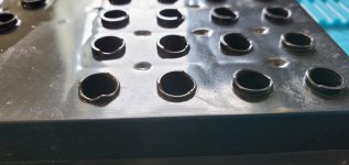
20230322_140254.jpg
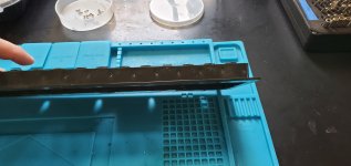
Hard to get on camera but a bit warped.

Its also missing a Shift key (one is coming) and a half a dozen springs.

Hopefully I can get it working... OK, I know I can get it working, hopefully I can get it pretty.

Mike
 
That's very strange damage, Mike, but on looking at it I am halfway convinced this is not actually heat damage.

The keys, made from plastic, would have had to have been dismounted when the hypothetical heat was applied otherwise they would have been in an even worse state / even more deformed. They don't look heat damaged at all.

The 'dimples' in between the key receptacles are probably from the original manufacturing process.

Putting my Sherlock Holmes deerstalker on, I notice that the 'lips' on those receptacles are mostly on the lower left edge on the keys on the left hand side of the keyboard - in other words, the receptacles for the keys which would mostly be struck with the left hand are deformed on their lower left edge, and the receptacles for the keys on the main keyboard which would mainly be struck with the right hand are deformed towards the lower right, and the receptacles of the separate keypad on the right, also likely to be struck with the right hand, are also deformed on the lower right. That is provided the moulding in your pictures is the way round that I think it is.

I'm wondering if this is some sort of 'hammer' damage caused by the keys repeatedly striking those circular ridges at the bottom of their travel with the location / direction of the damage biased by the hand most often used to strike them.

If there is anything in this theory we could expect that the most used keys / most used letters would be the ones with the most prominent damage, with rarely used letters like 'Z' having relatively little damage to the rim of the key receptacle. You also have to bear in mind, when considering this, which ones tended to be used in popular games, such as 'A' for Fire in Space Invaders.

The ASUS PC keyboard I'm using right now is about 13 years old and there is a conspicuous hollow in the plastic enclosure just below and left of the left end of the spacebar. I've never thought about why that is until now but I have just realised I have a habit of resting the tip of my left thumb in that spot while I am typing. Not rubbing, not pressing, just resting, and yet I have still managed to wear a small hollow in that spot.
 
That's very strange damage, Mike, but on looking at it I am halfway convinced this is not actually heat damage.

The keys, made from plastic, would have had to have been dismounted when the hypothetical heat was applied otherwise they would have been in an even worse state / even more deformed. They don't look heat damaged at all.

The 'dimples' in between the key receptacles are probably from the original manufacturing process.

Putting my Sherlock Holmes deerstalker on, I notice that the 'lips' on those receptacles are mostly on the lower left edge on the keys on the left hand side of the keyboard - in other words, the receptacles for the keys which would mostly be struck with the left hand are deformed on their lower left edge, and the receptacles for the keys on the main keyboard which would mainly be struck with the right hand are deformed towards the lower right, and the receptacles of the separate keypad on the right, also likely to be struck with the right hand, are also deformed on the lower right. That is provided the moulding in your pictures is the way round that I think it is.
That's an interesting point. I do think the dimples are normal but the rings where the keys go look wet. It may just be a poor quality mold that did not get enough material at manufacture!

Mike
 
There are some plastics that undergo conformational change with heating, and when heated the gaps in the molecular spaces can shrink and the volume of the plastic drops and its density and hardness increases. To check this theory out is simple, try to scratch the plastic on the rounded melted looking edges, if it is a lot harder than the plastic elsewhere, then this is likely what has happened.
 
There are some plastics that undergo conformational change with heating, and when heated the gaps in the molecular spaces can shrink and the volume of the plastic drops and its density and hardness increases. To check this theory out is simple, try to scratch the plastic on the rounded melted looking edges, if it is a lot harder than the plastic elsewhere, then this is likely what has happened.
Funny you should mention that. When I was a kid my dad was a Scuba Diver for the University and he had a Styrofoam cup that he had taken on a deeper dive that was about the size of a shot glass and strong enough for me to stand on.

As for the keyboard I did a test where the Shift key is missing and the plastic is quite soft. I think that Commodore was just being Commodore and they used this frame since it does still work. It turned out that the wonky keys had loose posts (They just press in?) and overall I was surprised how good it looks. Of course I still have to test it. After cleaning the carbon pads that I tested were all about 150 ohms.

20230324_175305.jpg
 
Last edited:
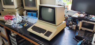
While waiting for parts i can at least assemble the cosmetically restored parts.

Is there any reason i shouldn't socket the rooms and ram while i wait? The pins are pretty rusty.
 

Attachments

  • 20230325_152513.jpg
    20230325_152513.jpg
    1 MB · Views: 1
OK The CRTCs came a few days early and I just tested it.

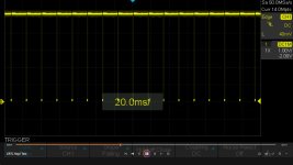
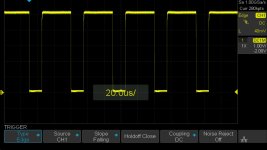
Now, I get good looking square waves on Pins 3 and 7 of J7 that look to match the timings shown on the schematic. Tomorrow I will install the VDU board in the pet and try for an image.

I changed the rusty SCR on the VDU board and cleaned it. Is there anything else I should check before first powering it? I know I read a TON of threads when I was on vacation but now I am having trouble finding all the sweet nuggets of goodness. I plan to go through them and make notes soon!

CRTC Test J7P3.jpg
J7 Pin 3 - 1V 20mS / Div

CRTC Test J7P5.jpg
J7 Pin 5 - 1V 20uS / Div

Mike
 
Well, no huge surprise. The heater is on in the neck but there is no image, nor is there any static or other signs of high voltage.

I'll start researching the VDU board. I remember there being mention of some resistors that go bad and some threads that cover this pretty well.

I am a digital guy so the analog and high voltage stuff is definitely not my bally-wack!

Mike
 
Back
Top