daver2
10k Member
Ah ha...
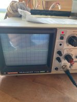
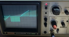
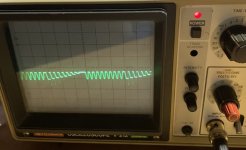
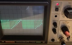
The change in Q503 collector corresponds to the brightness we see of the dot on the screen. This is good. I would have expected a greater voltage change myself - but the fact that we observe a change - and it is also being modulated with the Z-AXIS signal (this is - presumably - where the oscillating wave comes from) is very good. I can do a calculation later to verify what we are observing...
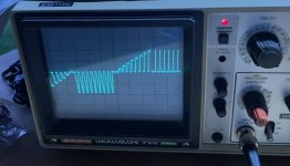
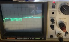
Q504 collector also has a healthy voltage swing now.
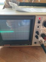
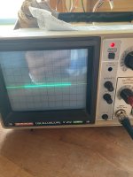
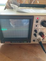
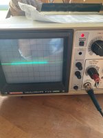
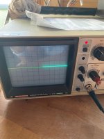
So the question now is why is the X and Y axis not deflecting correctly?
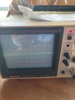
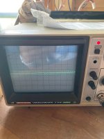
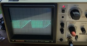
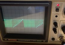
Back to checking the waveforms on both sides of R420 and R421 with your switch both OFF and ON.
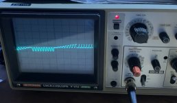
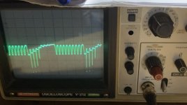
In both cases you should have healthy deflection signals on Q401 and Q402 source leads.
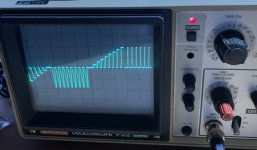
Q401 and Q402 drain leads should be similar to the source leads when the switch is in one state, and much reduced with the switch in the other state.
If you don't get any joy on the drain leads of Q401 and Q402, it may be worth checking the signals on the gate leads.
Dave
The change in Q503 collector corresponds to the brightness we see of the dot on the screen. This is good. I would have expected a greater voltage change myself - but the fact that we observe a change - and it is also being modulated with the Z-AXIS signal (this is - presumably - where the oscillating wave comes from) is very good. I can do a calculation later to verify what we are observing...
Q504 collector also has a healthy voltage swing now.
So the question now is why is the X and Y axis not deflecting correctly?
Back to checking the waveforms on both sides of R420 and R421 with your switch both OFF and ON.
In both cases you should have healthy deflection signals on Q401 and Q402 source leads.
Q401 and Q402 drain leads should be similar to the source leads when the switch is in one state, and much reduced with the switch in the other state.
If you don't get any joy on the drain leads of Q401 and Q402, it may be worth checking the signals on the gate leads.
Dave
Last edited:
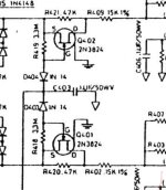
") First of all, I am not familiar with this kind of Transistor. But I guess when you talk about the source leads you mean what is shown in the schematic as S and D, right? Gate is probably G and Drain is the leg to ground?
First of all, I am not familiar with this kind of Transistor. But I guess when you talk about the source leads you mean what is shown in the schematic as S and D, right? Gate is probably G and Drain is the leg to ground?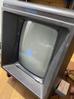
 .
.