• Please review our updated Terms and Rules here

Vectrex (newer version - no buzz) - Troubleshooting Sound but no Video

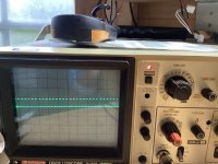
Hi, made some progress today. The sound is now working again. After hunting with my scope again and again I came to my limit without having the proper schematic. I simply did not know where the signal goes further.

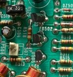
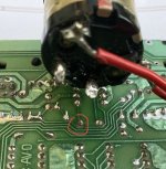
So, I de- installed the logic board again and followed the traces with my multimeter and magnifying glasses. And finally I found the culprit. There is a trace going to Pin3 of the amplifier chip (Sound input) and running very close to a capacitor I replaced a few months ago. I obviously slightly damaged the trace while removing the cap (desoldering gun too hot?). Not really visible on the glance. Arrgh :mad:

I did install a bodge wire and put the system back together. Now MineStorm is running with sound. Hurrah 😁

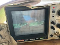
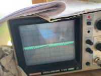
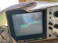
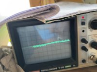
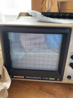
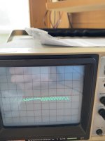
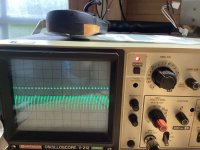
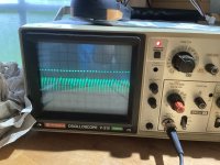
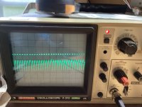
Next problem solved. Now I will hunt for the missing video. I guess I will look to the transistors I mentioned above.

Cheers
Denis
 

Attachments

  • IMG_9292.jpeg
    IMG_9292.jpeg
    636.4 KB · Views: 8
Nice job with the audio. Yes, damage to the PCB that is self inflicted really needs to be assessed at the point of doing the work. It is always best to leave your repair for a day and then to look at your previous day's work critically the following day.

Let me have another think about the video.

There is a protection circuit that monitors the activity of the Y deflection (I think) and shuts off the video if nothing has changed within a period of time. This acts to protect the CRT from screen burn if the CPU fails. Of course, if the protection circuit fails - you will get a blank screen for no reason...

Dave
 
There are two (2) things that must be satisfied before you get brightness on the screen.

These references are (obviously) based upon the 'wrong' schematic...

The Z-AXIS signal drives Q505.

The Y-AXIS monitoring drives Q503 (via C409).

I 'think' both transistors have to be conducting to bright-up the CRT spot.

Dave
 
Thank you Dave. Thats very helpful.

In post #50 I reported “can clearly see the Z-Axis Signal going in (Q505-B) and coming out (Q505-E)”. So I will focus on Q503 first. I am gonna unsolder the transistor and test with my component tester. This should give me an idea, hopefully. I already looked for shorts on these transistors between all legs but could not found any.

Unfortunately I am on travel until Sunday so the old Vectrex needs to wait😉

Will give an update asap.

Have a nice evening 🖖
 
I can understand the signal going 'into' Q505 base. What do you mean 'coming out of Q505 emitter'?

You should also be able to look at the signal on Q503 base and on Q505 collector / Q503 emitter. All relative to 0V/GND.

Yea, I know what you mean about travelling...

Dave
 
Hi Dave, maybe I am not quite understand the schematic thinking the emitter is the output of that transistor ?!

However, today I desoldered Q303, Q304 and Q305 and checked them with my component tester. The tool detected the right type of transistor on each one. They all look ok from my point of view…
 
I think IC401 is the next thing to check. Have not done this yet. The Troubleshooting Manual gives some directions how to scope at Pin 7 and 8 and how the waveform should look like….
 
A transistor amplifies a small current flow between the base and emitter so that a larger current flows between the emitter and collector. Therefore, to say that the emitter is the transistor output is not correct. It may seem it from the arrow possibly, but this just indicates (a) the emitter pin and (b) the type (NPN or PNP).

Did you check the voltage on the base of Q503 as I asked (relative to 0V)? Q503 (and the associated circuitry) monitors the Y deflection output from IC401 and shuts off the beam if no movement is detected.

You can easily check IC401 (and the associated circuitry) by monitoring pins 5 and 10. These may be difficult to get to (because of the heatsink) so the easier points may be the green and red wires from the Power PCB to the deflection coils. If there are signals here, then all is fine. If not, work backwards to see where the signal appears.

What signal are you getting on Q503 collector? This drives the tube cathode and controls the beam on/off.

Dave
 
Understand. Thank you.

Yes, I measured the VDC at the Q503 Base and I read 0,3 mV. The signal at the collector is static 49,6V. There is no waveform whatsoever.

i can easily reach the IC401 from the solder side and pin1 is marked up. There is no activity on Pin 5 and 10. Just a little static voltage (-100mV and -70mV).

There is also no activity on Pins 7 and 8 following the advice in the troubleshooting manual and using the test cart.

looks not right I guess.:( Maybe IC401 is faulty?
 
0.3 mV at the base of Q503 is not correct. However, if there is no deflection of the X or Y axis, this is to be expected!

Give me a second to check the schematics again...

EDIT:

If there is no signal coming out of IC401 on pins 5 and 10, but there is also no signal going INTO IC401 on pins 7 and 8, then it is unlikely that IC401 is actually faulty (as a first assumption). If there was a signal going in and nothing coming out, then this would be a possibility (after we have checked the power pins of course). This is not the case here.

Can you just double check that you have a signal on EP401 (X), EP403 (Y) and EP506 (Z) and that we are not chasing our tails...

Dave
 
Last edited:
I really looked to these Pins multiple times and always found the waveforms for X,Y and Z.
I can scope there again tomorrow and will check the Input Pins on IC401 on more time just in case I did not set my scope properly…
 
If the signals are there on the pins, that is good.

The next point to check will be the signal on the wiper of the XSIZE and YSIZE trimmer resistors on the board. We then work our way forwards through the schematic (from left to right) until we loose the signals...

Dave
 
If the collector of Q503 is positive - then the CRT is biased OFF.

The CRT will be biased ON if transistor Q503 is conducting (there is some Y deflection) AND the Z-AXIS is switched ON (Q505 is conducting).

The combination of both Q503 and Q505 conducting will pull down the CRT cathode voltage from the +49.6 Volts you are reading to a very low value - and the CRT spot should illuminate.

There is another transistor (Q504) which operates to inhibit (or reduce the amplitude of) the deflection amplifiers (I am not sure which yet).

After double checking the signals in post #70, can you also look at the signals on both sides of resistors R420 and R421 (both 47k) relative to 0V. I suspect this is where the deflection signals may be disappearing...

Dave
 
Last edited:
Hi Dave

Thank you very much for all of your input.:)

Today I followed the traces for X and Y. Measuring at EP401 (X), EP403 (Y) and EP506 (Z) confirmed that I get still good signals there. Perfect waveforms and they all match the pictures in the troubleshooting manual. Good.

I have checked the X SIZE and Y SIZE potis and found my waveforms on all contacts. Looks good.

Then I looked at R420 and R421 on both sides. Took me a while to find the solder points on the solder side of the board. These resistors are completely hidden below the big heatsink. But using the Component layout and following the traces helped me finding these resistors. These inputs looked ok but the outlet is as bit pulled below 0. Please have a look to my screenshots. I adjusted the sweep to 0 before I start scoping.
Hmm. Not sure whether thats normal.

Then I looked to the next resistors (R402, R409). These are just before IC401. The input there match the output of the previous resistors (R420, R421) of course. But after them there is no waveform anymore. It´s just pulled below 0. There I loose the signals. Both. See my pictures.

I guess the IC401 is pulling them down?! Bad Chip probably?
 

Attachments

  • R420 IN - Q401-S.jpeg
    R420 IN - Q401-S.jpeg
    1.1 MB · Views: 1
  • R420 OUT - Q401-D.jpeg
    R420 OUT - Q401-D.jpeg
    873.9 KB · Views: 1
  • R421 IN - Q402-S.jpeg
    R421 IN - Q402-S.jpeg
    1,011 KB · Views: 1
  • R421 OUT - Q402-D.jpeg
    R421 OUT - Q402-D.jpeg
    1.1 MB · Views: 1
  • R409 IN.jpeg
    R409 IN.jpeg
    1.1 MB · Views: 1
  • R409 OUT - IC401-8.jpeg
    R409 OUT - IC401-8.jpeg
    1 MB · Views: 1
  • R402 IN.jpeg
    R402 IN.jpeg
    923.6 KB · Views: 1
  • R402 OUT - IC401-7.jpeg
    R402 OUT - IC401-7.jpeg
    893 KB · Views: 1
Why do you keep thinking it is IC401 that is faulty?

You are fixated on this!

The transistors Q401 and Q402 would be switched ON under normal circumstances, thus the two 'sides' of R420 and R421 will have very similar signals on them (i.e. Q401 and Q402 are switched ON and - effectively - short out R420 and R421). When Q401 and Q402 are switched OFF, R420 and R421 are in circuit - thus significantly reducing the drive signal to the deflection amplifier IC401.

Q401 and Q402 are switched ON and OFF by a signal from our favourite Q503, Q504 and Q505 transistors via R518.

If you check the signal on either side of R518 next and C405 please.

If I am correct, the deflection system is acting to protect itself (possibly from an imaginary fault). We then just have to work out why...

Dave
 
Hi Dave, I don’t know why I am so fixated to IC401. It’s just a feeling without understanding the circuits around it. Not the right approach I know :(

I have checked R518. There is no waveform found on either side and I measured -19 VDC on both pins.
Also no waveform at C504. I measured 0,0 VDC on the ground side as expected and on the other side -265 mV.

is that what you expected?

Sorry for my late replies to your recent posts. I was seldom at Home and thus unable to follow up. It’s better today and next week 😊
 
So, -19VDC on R518 indicates that the transistors Q401 and Q402 are being told to switch OFF - hence attenuating the signal of both the X and Y deflection to IC401 (no, it isn't faulty - just to reiterate)... Well, not at the moment at least!

We need a positive voltage on R518 to switch the transistors Q401 and Q402 ON, and restore normal operation...

I may have given you a faulty capacitor number to check. According to the schematic I have in front of me it should have been C409. This should be a NON POLARISED capacitor. One end of C409 should be connected to R417 (100 Ohms) to make sure I get the correct capacitor this time... Please make sure this is a NON POLARISED capacitor.

I know you are going to hate me, but I think the problem is within Q503, Q504 or Q505 or the associated circuitry somewhere. Can you measure (using your oscilloscope) the voltages on:

Q503 collector and emitter.
Q504 collector and emitter.
Q505 collector and emitter.

I also see two (2) things I have never seen on the schematic before - FB501 and FB502. What are these things? EDIT: I think they are little ferrite beads (FB) applied to the emitters of Q503 and Q504.

With the power OFF, can you check for continuity between the following pairs of points:

Q503 emitter and Q505 collector.
Q505 collector and Q504 emitter.

>>> Sorry for my late replies to your recent posts.

Absolutely no problem whatsoever. It gives us both time to think...

Dave
 
Last edited:
Hi Dave,

found the capacitor C409 and indeed it is connected to R417 and it is non-polarized for sure. Looked with my scope and measured the voltage on both sides: Pin connected to R417: - 0,06 VDC and the other side is 0,00 VDC

I am not complaining re- checking these 3 transistors again. Actually I got a different opinion since I watched one of the recent Adrian Black Videos where he found a faulty transistor in an Apple 2 which he tested in a component tester ok (like I did with Q503,504,505) but replacing that thing solved his problem. After watching this video I ordered replacement for all 3 transistors just in case....

So, here are my results:

Q503 collector: static 52 VDC, no waveform / emitter: waveform see photo
Q504 collector: static -19,1 VDC, no waveform / emitter: waveform see photo
Q505 collector and emitter: see waveform photos

I was very carefully not to mix Emitter, Base and collector while measuring from the solder side and being aware that the pinout between these 3 transistors are different. I checked the datasheets before.

I have checked continuity as you asked for and it is all good.

FB501 and FB502 are ferrite cylinders according the manual. Not sure what´s the purpose of these. Found FB502 on a photo when I got my first Vectrex on the bench. Looks just like a trace here...
 

Attachments

  • Q505-E.jpeg
    Q505-E.jpeg
    1.6 MB · Views: 5
  • Q505-C.jpeg
    Q505-C.jpeg
    1.7 MB · Views: 4
  • Q504-E.jpeg
    Q504-E.jpeg
    1.4 MB · Views: 3
  • Q503-E.jpeg
    Q503-E.jpeg
    1.5 MB · Views: 3
  • FB502.jpg
    FB502.jpg
    77.4 KB · Views: 5
Excellent, I will check when I get home from from my walk. It has suddenly got hot in the UK again today, and it is forecasted to stay for the week...

I added the information in my post above regarding the ferrite bead. They are there to suppress 'noise'. The transistor lead is a 'half transformer winding' and the ferrite bead acts as a ferrite core.

Dave
 
Oh yes, like in Germany. The summer comes back ;)
Take your time. Thanks for your help and have a nice evening.
 
Back
Top